Prototyping Board Design
I do all of my PCB design work using Eagle CAD (the free version, so there are limitations, but everything I've done fits within these limitations). The basis for my original prototyping work was simply a standard 100mil breadboard matrix on PCBs that fit into common 100mm x 68mm (34 x 22 matrix) and 85mm x 58mm (28 x 18 matrix) enclosures.
Eagle CAD Files
The CAD work uses two fundamental elements, the pad matrix and the board outline, and these are combined to provide a base for all of my prototyping boards.
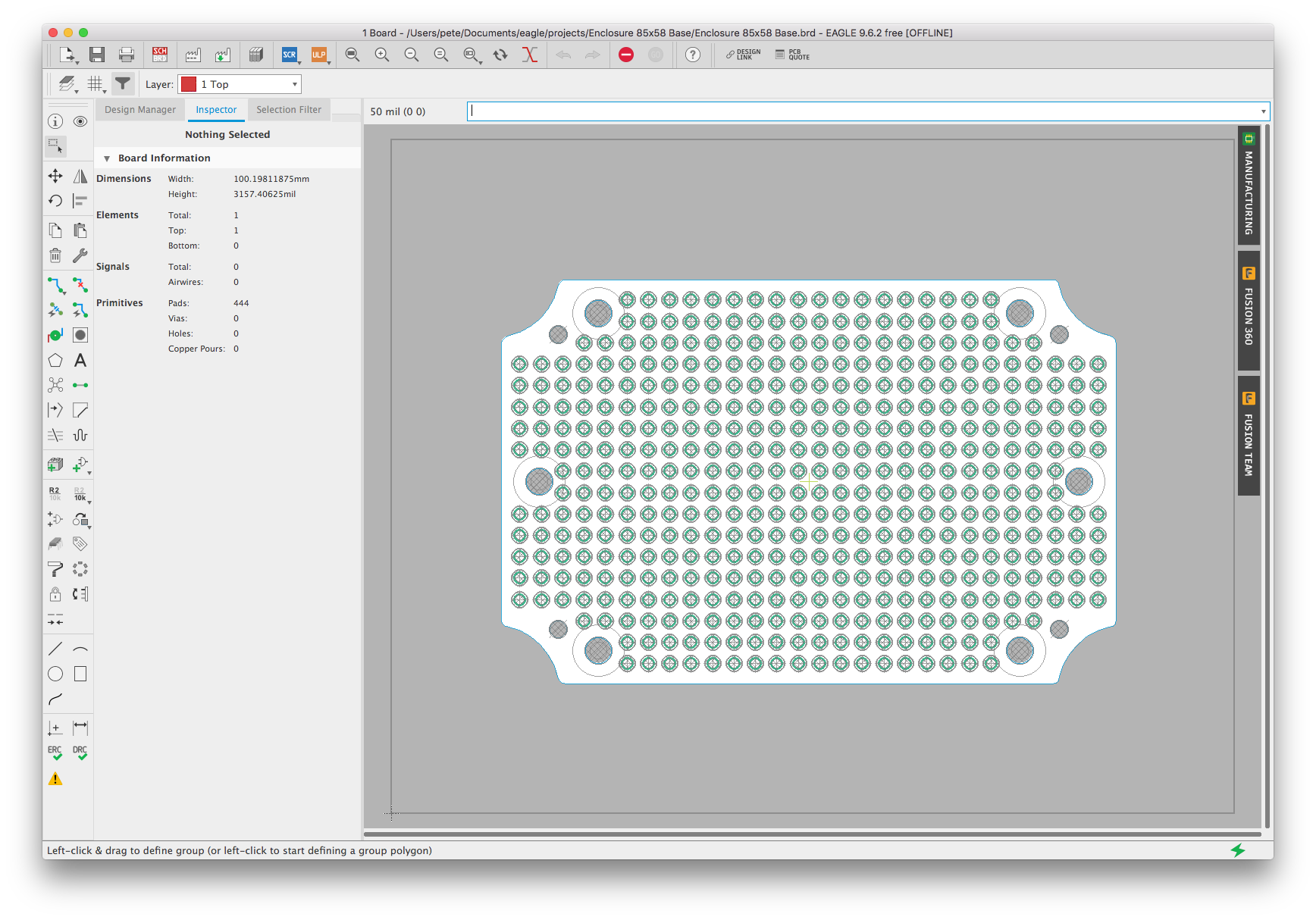
85mm x 58mm Enclosure
Pad Matrix (28 x 18)
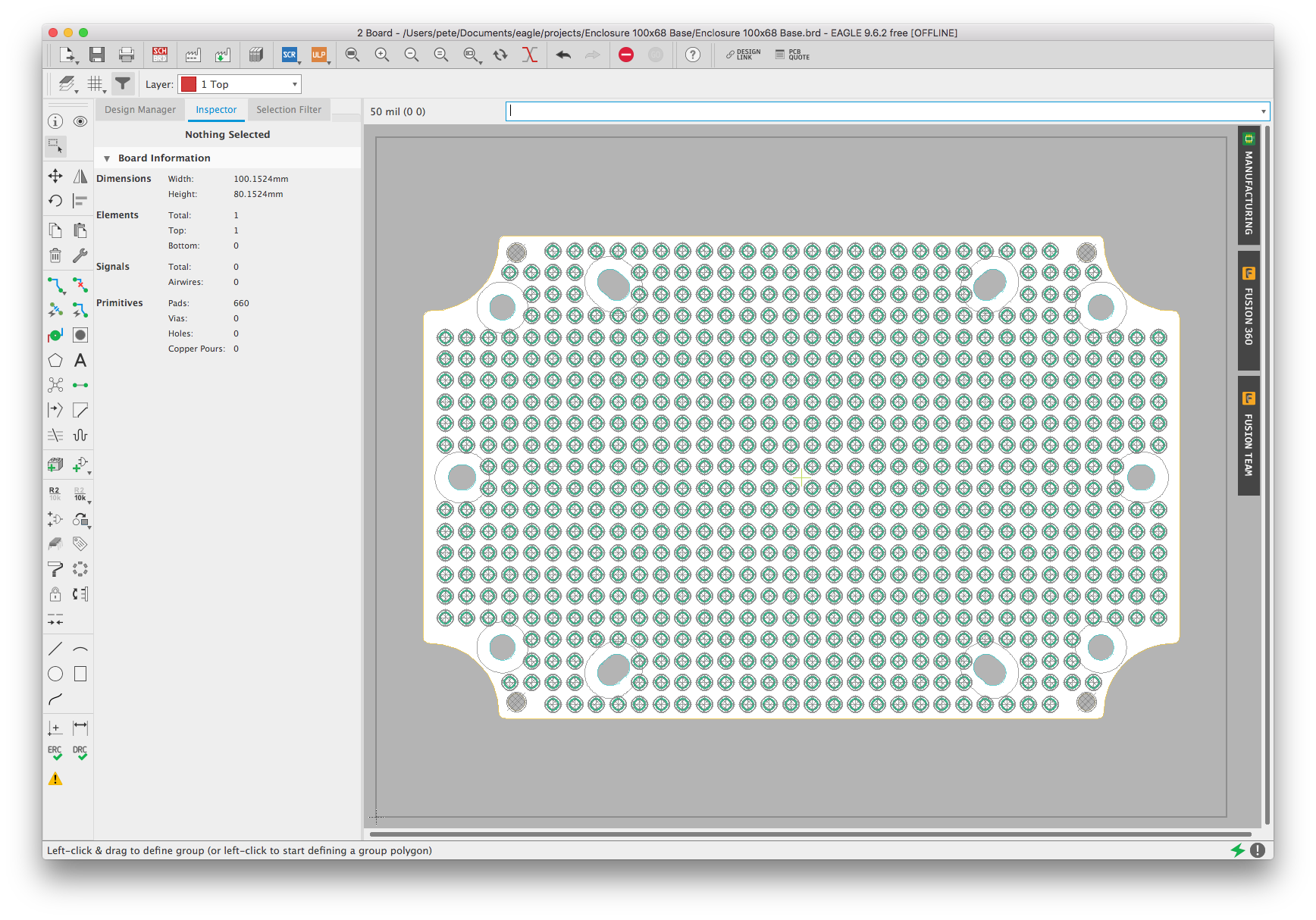
100mm x 68mm Enclosure
Pad Matrix (34 x 22)
I have saved the two basic pad matrices, footprints for the relevant battery holders and the ALF4all 'Sandwich' boards in an Eagle library file (dcprotoboards.lbr) that can be downloaded via the following link:

|
Eagle Prototyping Device Library Archive | [67 KB] |
Enclosures
I have used three different types of 100mm x 68mm enclosure—a plain enclosure with 6 mounting posts and four support pins that is 50mm high (below left), an enclosure with a clear cover, 6 mounting posts and flanges with two mounting holes each that is also 50mm high (below centre), and an enclosure with a clear cover, 10 mounting posts and flanges with a single mounting hole in each that is 40mm high (below right):
The number of mounting posts notwithstanding, the enclosures appear very similar internally, but the post spacings are slightly different. To manage this situation, the prototyping boards for the 100mm x 68mm enclosure include mounting slots, rather than holes, that cover the extent of variation in post locations that I have encountered to date. The silkscreens on the reverse side of the boards also include an outline of the mount point 'posts' to indicate the area that should remain clear of any obstruction.
The Eagle CAD library also includes a [100mm x 68mm] board with mounting holes for a Raspberry Pi Zero. This is no big deal, it's easy to add the holes, but since I had it I included it.
I prefer to use the 10-post enclosure with the smaller flanges and single mounting hole (above at right) because it is slightly more compact, at 40mm rather than 50mm high, a little more flexible in terms of mounting screw location and the manufacturing quality is better. It's not as widely available and tends to be a little more expensive, but [at the time of writing] we're only talking about A$5.30 vs A$5.80. If you're looking for a source, follow the link in the opening paragraph above for the AliExpress store that I have used, or just search in general for a 100x68 enclosure— the 50mm high versions, with or without flanges, clear or solid cover, are available from any number of suppliers.
Creating a Bounding Box
The free version of Eagle CAD restricts the board size to 100mm x 80mm (width x height—you cannot, for example, work on a board that is 80mm x 100mm). To make this boundary clear, I find it convenient to create a bounding box in new .brd files. To do this, execute the following commands from the Eagle CAD command line:
- grid mm
- layer tDocu
- wire (0 0)(100 0)(100 80)(0 80)(0 0)
This will create a bounding box like the ones you can see [in grey] in the Pad Matrix images above.
Using a Matrix Footprint
To use a pad matrix:
- Download the Eagle Prototyping Library archive (see above)
- Extract the dcprotoboards.lbr file and save it to a convenient location (e.g. in the Eagle libraries folder)
- Within Eagle CAD, open your project, select Add Part from the left side Tools Palette, navigate to this library and insert the PROTO-28x18 or PROTO-34x22 device in a convenient location in your schematic—there are no connections, so it just needs to sit there somewhere
The way I then work with these matrices when designing a new layout is to:
- In the library editor, duplicate the required footprint (PROTO-28x18 or PROTO-34x22)
- Also in the library editor, create a new device using this footprint and the PROTO-MATRIX symbol (or any symbol you like)
- Add this device to the schematic for the new board;
- Open the relevant footprint in the library editor and keep that window open next to the window for the new board layout
- As you add components to the new board, delete any pads necessary to make space for the new components from the matrix footprint in the library editor, save the modified footprint and reload the device in your schematic—the updated footprint should then show up in your board layout
For ease of identification and location on the boards, all of the pads in the matrices are numbered by row and column, in the format Prr-cc (e.g. Pad P06-14 is located in the 6th row and 14th column). Unfortunately, I started with my matrices in portrait mode (long side vertical) before discovering that they would not fit, in that orientation, within the bounds set for the free version of Eagle CAD. As a consequence, the logic of the row/column numbering in the current landscape orientation might not be immediately obvious—in this mode, the row numbers (the first two digits) actually refer to the columns, numbered from left to right, and the column numbers (the second two digits) refer to the rows, numbered from bottom to top.
PCB Serial Numbers
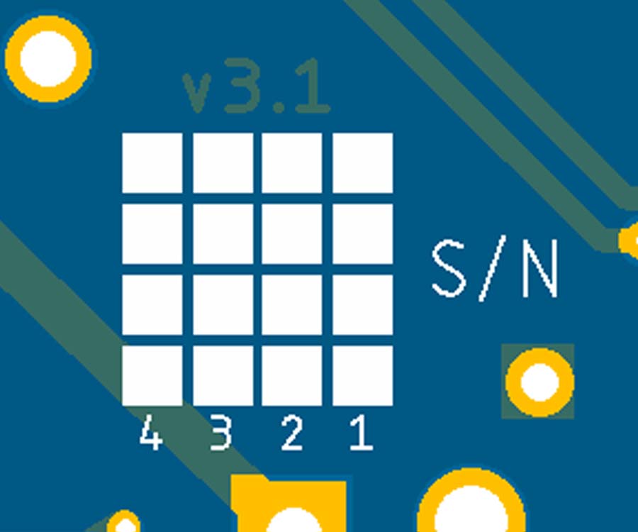
This didn't matter all that much initially but, as the number of boards I made started to add up, it became more important to know what features, and perhaps more importantly what faults, were present on a particular board. After a brief search for an appropriate solution, I settled on the present approach, which includes a 4 x 4 pad of squares on the PCB silkscreen that can be marked (just by hand) to encode a four hexadecimal digit number.

This allows the identification of 4096 boards in any sequence (if there is a need for more, one need only add more columns to the matrix). If this number is then prefixed by the PCB revision number, we can uniquely identify 4096 boards of any individual revision.
Since it is invariant for any production run, the PCB revision number is etched into the copper layer, adjacent to the serial number pad matrix.
Using a four-digit encoding (0301) of the PCB revision number (v3.1 in the present example) as a prefix, and the matrix marking illustrated, we get the following eight hex digit serial number:


