

Espressif ESP32
- Espressif ESP32
- Elecrow ESP32 WiFi/BLE Board
- Heltec WiFi LoRa 32 (V1, V2, V3 & V4)
- Heltec Wireless Stick Lite (V1 & V3)
Pin Definitions
Espressif ESP32
This article, from Random Nerd Tutorials, provides a good overview of the ESP32 processor and associated pin usage.
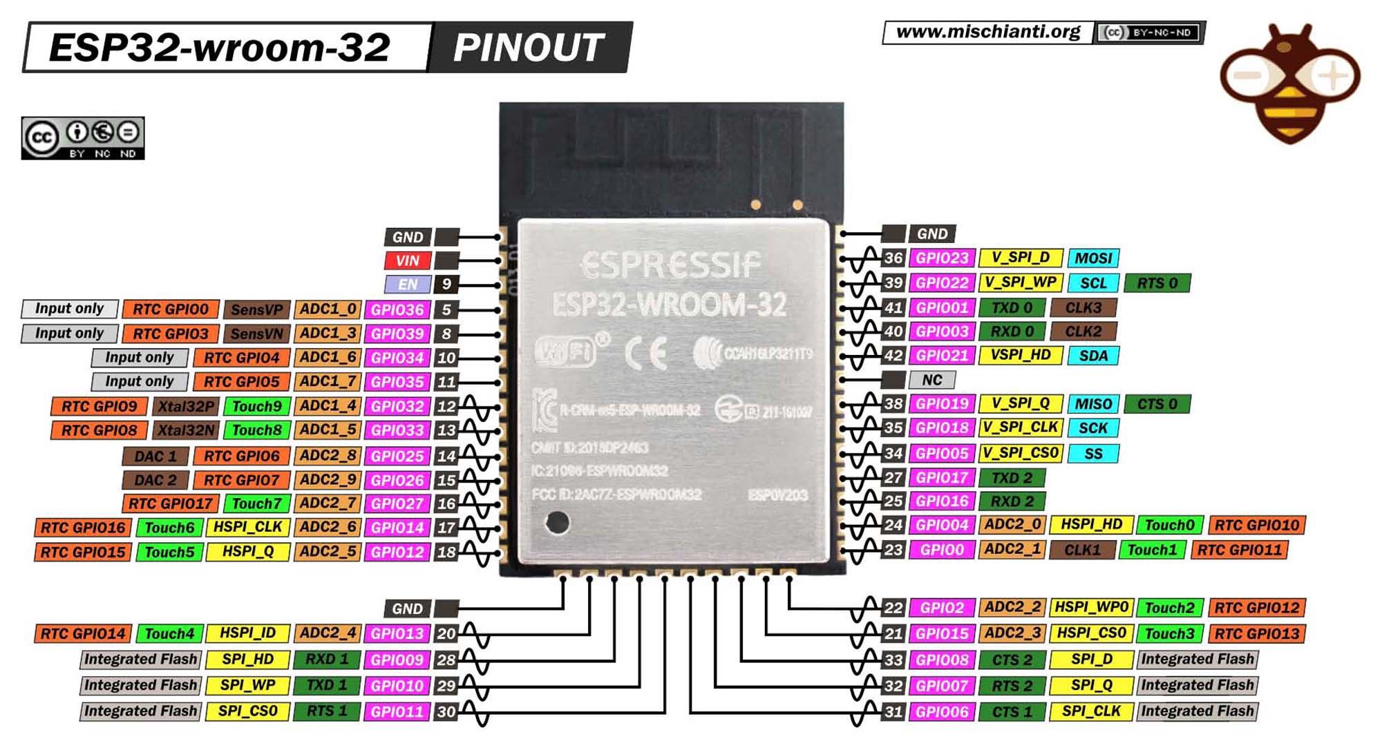
The ESP32-WROOM-32 pin functions are presented in the following pinout diagram.
1 2 3 4 5 6 7 8 9 10 11 12 13 14 15 16 17 18 19 20 21 22 23 24 25 26 27 28 29 30 31 32 33 34 35 36 37 38 39 40 41 42 43 44 45 46 47 48 49 50 51 52 53 54 55 56 57 58 59 60 61 62 63 64 65 66 67 68 69 |
#define Builtin_LED2
#define GPIO00 #define GPIO11 #define GPIO22 #define GPIO33 #define GPIO44 #define GPIO55 #define GPIO66 #define GPIO77 #define GPIO88 #define GPIO99 #define GPIO1010 #define GPIO1111 #define GPIO1212 #define GPIO1313 #define GPIO1414 #define GPIO1515 #define GPIO1616 #define GPIO1717 #define GPIO1818 #define GPIO1919 #define GPIO2121 #define GPIO2222 #define GPIO2323 #define GPIO2525 #define GPIO2626 #define GPIO2727 #define GPIO3232 #define GPIO3333 #define GPIO3434 #define GPIO3535 #define GPIO3636 #define GPIO3939 #define CLKGPIO6 #define CMDGPIO11 #define SD0GPIO7 #define SD1GPIO8 #define SD2GPIO9 #define SD3GPIO10 #define SVNGPIO39 #define SVPGPIO36 #define U0RXGPIO1 #define U0TXGPIO3 // SPI (RFM95W) #define SCKGPIO18 #define MISOGPIO19 #define MOSIGPIO23 #define NSSGPIO5 #define RSTGPIO14 #define DIO0GPIO26 #define DIO1GPIO33 #define DIO2GPIO32 // I2C #define SDAGPIO21 #define SCLGPIO22 // ALF4all #define A4a_A0GPIO36 #define A4a_A1GPIO13 #define A4a_A2GPIO17 #define A4a_A3GPIO27 |
Elecrow ESP32 WiFi/BLE Board
The ESP32 (ESP32-WROOM-32) WiFi/BLE Board pin functions, which are simply those of the standard ESP32 DevKit board, are presented in the following pinout diagram.

1 2 3 4 5 6 7 8 9 10 11 12 13 14 15 16 17 18 19 20 21 22 23 24 25 26 27 28 29 30 31 32 33 34 35 36 37 38 39 40 41 42 43 44 45 46 47 48 49 50 51 52 53 54 55 56 57 58 59 60 61 62 63 64 65 66 67 68 69 70 71 72 73 74 75 76 77 |
// Most pins on the ESP32 WiFi/BLE Board are physically
// numbered according to their ESP32 pin identifiers #define Builtin_LED16 #define GPIO3636 #define SVP36 #define GPIO3939 #define SVN39 #define GPIO3434 #define GPIO3535 #define GPIO3232 #define GPIO3333 #define GPIO2525 #define GPIO2626 #define GPIO2727 #define GPIO1414 #define GPIO1212 #define GPIO1313 #define GPIO99 #define SD29 #define GPIO1010 #define SD310 #define GPIO1111 #define CMD11 #define GPIO2323 #define GPIO2222 #define GPIO11 #define U0RX1 #define RX1 #define GPIO33 #define U0TX3 #define TX3 #define GPIO2121 #define GPIO1919 #define GPIO1818 #define GPIO55 #define GPIO1717 #define GPIO1616 #define GPIO44 #define GPIO00 #define GPIO22 #define GPIO1515 #define GPIO88 #define SD18 #define GPIO77 #define SD07 #define GPIO66 #define CLK6 //RFM95 (via SPI) #define SCKGPIO18 #define MISOGPIO19 #define MOSIGPIO23 #define NSSGPIO5 #define CSGPIO5 #define RSTGPIO14 #define DIO0GPIO26 #define DIO1GPIO33 #define DIO2GPIO32 // I2C #define SDAGPIO21 #define SCLGPIO22 #define OLED_SDASDA #define OLED_SCLSCL #define OLED_RSTGPIO16 // ALF4all #define A4a-A0GPIO36 #define A4a-A1GPIO13 #define A4a-A2GPIO17 #define A4a-A3GPIO27 |
Heltec WiFi LoRa 32 (V1)
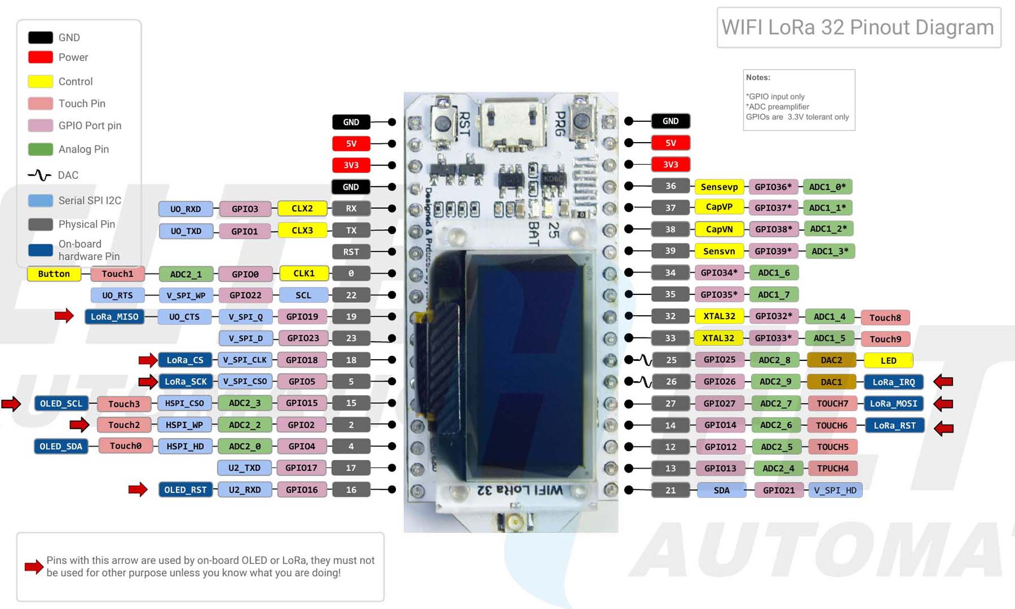
The WiFi LoRa 32 (V1) pin functions are presented in the following pinout diagram. Note that the Heltec boards do not use the ESP32-WROOM-32 processor module. As such, there are some GPIOs available on these boards, notably GPIO37 and GPIO38, that are not broken out on the ESP32-WROOM-32 or boards based on that processor module.
1 2 3 4 5 6 7 8 9 10 11 12 13 14 15 16 17 18 19 20 21 22 23 24 25 26 27 28 29 30 31 32 33 34 35 36 37 38 39 40 41 42 43 44 45 46 47 48 49 50 51 52 53 54 55 56 57 58 59 60 61 62 63 64 |
// Most pins on the WiFi LoRa 32 module are physically
// numbered according to their logical pin number #define Builtin_LED25 #define GPIO00 #define GPIO11 #define GPIO22 #define GPIO33 #define GPIO44 #define GPIO55 #define GPIO1212 #define GPIO1313 #define GPIO1414 #define GPIO1515 #define GPIO1616 #define GPIO1717 #define GPIO1818 #define GPIO1919 #define GPIO2121 #define GPIO2222 #define GPIO2323 #define GPIO2525 #define GPIO2626 #define GPIO2727 #define GPIO3232 #define GPIO3333 #define GPIO3434 #define GPIO3535 #define GPIO3636 #define GPIO3737 #define GPIO3838 #define GPIO3939 #define TXGPIO1 #define RXGPIO3 // SPI (LoRa) #define SCKGPIO5 #define MISOGPIO19 #define MOSIGPIO27 #define CSGPIO18 #define NSSGPIO18 #define RSTGPIO14 #define DIO0GPIO26 #define IRQGPIO26 // I2C #define SDAGPIO21 #define SCLGPIO22 #define OLED_SDAGPIO4 #define OLED_SCLGPIO15 #define OLED_RSTGPIO16 // ALF4all #define A4a-A0GPIO36 #define A4a-A1GPIO13 #define A4a-A2GPIO17 #define A4a-A3GPIO23 |
Heltec WiFi LoRa 32 (V2)
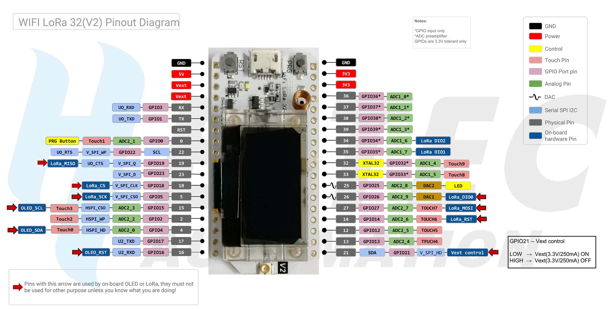
The WiFi LoRa 32 (V2) pin functions vary slightly from those of the V1 board, primarily in the configuration and ability to control the Vext [software activated] power supply pins. For some reason, the logic of which escapes me, Heltec decided to use GPIO21, the pin traditionally assigned to the I2C SDA function, to control the state of the Vext pin and measurement of the battery voltage. This basically meant that in order to use the switchable Vext pin, or to read the battery voltage, the I2C bus could no longer use its default pin assignment. The internal functions originally assigned to GPIO32 & GPIO33 were also moved to GPIO34 & GPIO35 respectively to avoid a conflict with channels used when WiFi was being used. The revised assignments are presented in the following pinout diagram.
The WiFi LoRa 32 (V2) variant was somewhat short-lived, replaced not long after its release by the V2.1 variant. I didn't ever have a V2 board, so I have never prepared a pin definition file for one.
Heltec WiFi LoRa 32 (V2.1)
The external pin functions of the WiFi LoRa 32 (V2.1) are the same as those of the V2 board but are nonetheless presented in the following pinout diagram. Note, however, that the internal functions of GPIO13 and GPIO37 have changed with this revision.
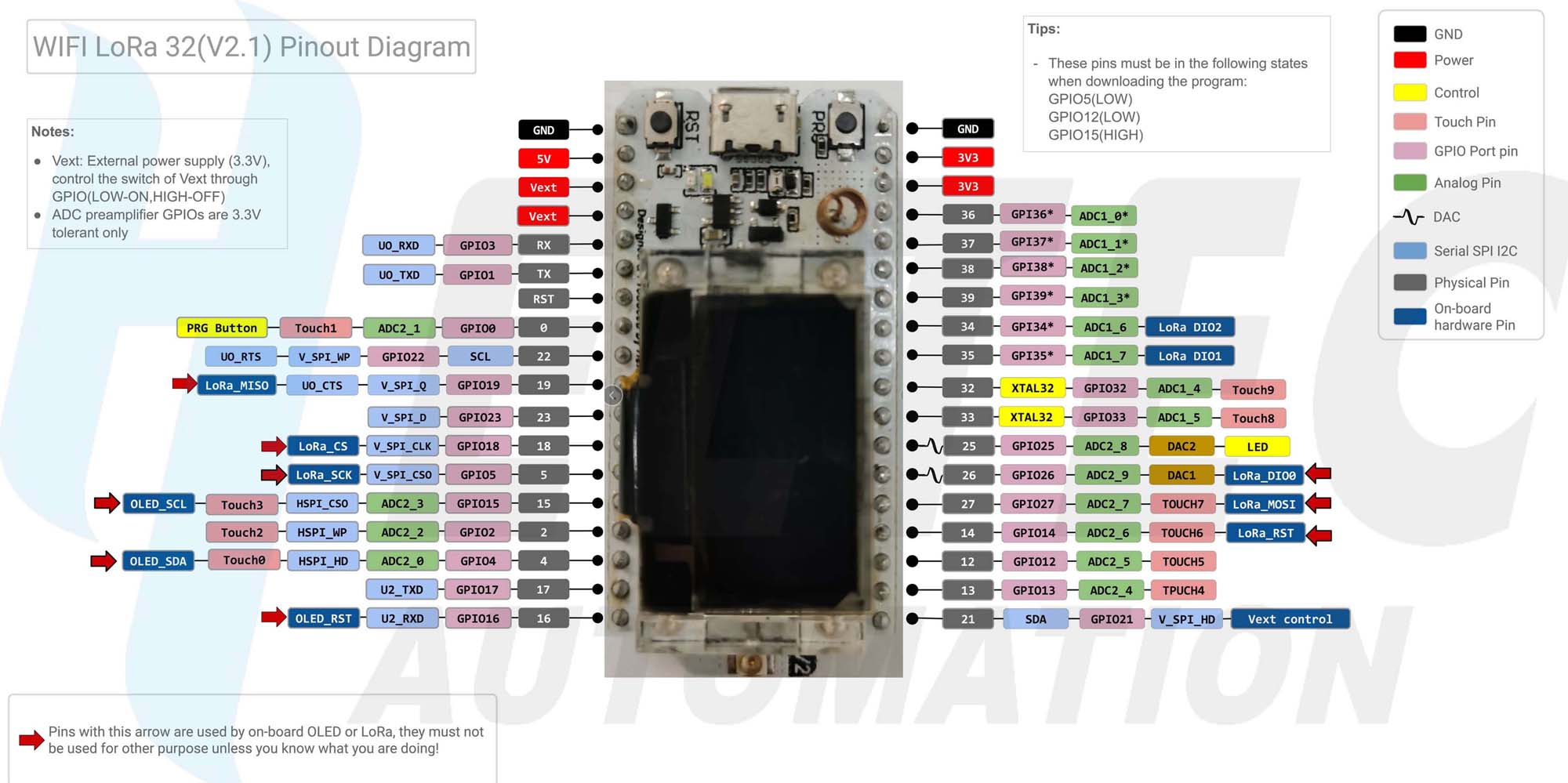
The main difference between the V1 and V2 boards was the inclusion of Vext [software activated] power supply pins. The change from V2 to V2.1 was made to circumvent internal conflicts with pin functions in the original V2 board design.
1 2 3 4 5 6 7 8 9 10 11 12 13 14 15 16 17 18 19 20 21 22 23 24 25 26 27 28 29 30 31 32 33 34 35 36 37 38 39 40 41 42 43 44 45 46 47 48 49 50 51 52 53 54 55 56 57 58 59 60 61 62 63 64 |
// Most pins on the WiFi LoRa 32 V2.1 module are physically
// numbered according to their logical pin number #define Builtin_LED25 #define GPIO00 #define GPIO11 #define GPIO22 #define GPIO33 #define GPIO44 #define GPIO55 #define GPIO1212 #define GPIO1313 #define GPIO1414 #define GPIO1515 #define GPIO1616 #define GPIO1717 #define GPIO1818 #define GPIO1919 #define GPIO2121 #define GPIO2222 #define GPIO2323 #define GPIO2525 #define GPIO2626 #define GPIO2727 #define GPIO3232 #define GPIO3333 #define GPIO3434 #define GPIO3535 #define GPIO3636 #define GPIO3737 #define GPIO3838 #define GPIO3939 #define TXGPIO1 #define RXGPIO3 #define ADC_CtrlGPIO21 #define VBAT_ReadGPIO37 // SPI (LoRa) #define SCKGPIO5 #define MISOGPIO19 #define MOSIGPIO27 #define CSGPIO18 #define NSSGPIO18 #define RSTGPIO14 #define DIO0GPIO26 #define IRQGPIO26 // I2C #define SDAGPIO4 #define SCLGPIO15 #define OLED_SDAGPIO4 #define OLED_SCLGPIO15 #define OLED_RSTGPIO16 // ALF4all #define A4a-A0GPIO36 #define A4a-A1GPIO13 #define A4a-A2GPIO17 #define A4a-A3GPIO23 |
Heltec WiFi LoRa 32 (V3)
The pin configuration of the WiFi LoRa 32 (V3) dev-board, presented in the following pinout diagram, is entirely different to the previous versions described above. Unlike the earlier versions, which were all based on the ESP32-D0WDQ6 MCU and SX1267 LoRa node IC, it is based on the ESP32-S3FN8 MCU and SX1262 LoRa node IC. In the present context then, this is effectively a completely new board, as it is not pin compatible with any other described on this website—I will have to design a completely new base board to specifically support this version.
The ESP32-S3 MCU is Espressif's current top-of-the-range SoC. The most obvious practical difference between this and previous versions of the ESP32 MCU would appear to be that it offers more GPIO pins (GPIO40–GPIO48). No doubt there'll be more discussion within the 'Arduino community' in relation to other differences as applications using this processor are developed.
In the past, Heltec has discontinued superseded versions of their dev-boards so it is likely that earlier versions will only be available 'while stocks last' and I will have to design some new boards in the near future.
I took the basic pin definitions below from the pins_arduino.h file included with the 0.0.7 release of the Heltec board software. Unfortunately, some of these assignments, the SPI pins used for LoRa communications in particular, are not consistent with the V3 board schematic. Fortunately, the LoRa radio SPI pin assignments are managed automatically when using the Heltec LoRaWan_APP library and, whatever they are, they work. In the mean time, the reader should use any of the SPI interface pins identified below with a degree of caution.

1 2 3 4 5 6 7 8 9 10 11 12 13 14 15 16 17 18 19 20 21 22 23 24 25 26 27 28 29 30 31 32 33 34 35 36 37 38 39 40 41 42 43 44 45 46 47 48 49 50 51 52 53 54 55 56 57 58 59 60 61 62 63 64 65 66 67 68 69 70 71 72 73 74 75 76 77 78 79 80 81 82 83 84 85 86 87 |
// Most pins on the WiFi LoRa 32 V3 module are physically
// numbered according to their logical pin number #define Builtin_LED35 #define GPIO00 #define GPIO11 #define GPIO22 #define GPIO33 #define GPIO44 #define GPIO55 #define GPIO66 #define GPIO77 #define GPIO1010 #define GPIO1111 #define GPIO1212 #define GPIO1313 #define GPIO1414 #define GPIO1919 #define GPIO2020 #define GPIO2121 #define GPIO2626 #define GPIO3333 #define GPIO3434 #define GPIO3535 #define GPIO3636 #define GPIO3737 #define GPIO3838 #define GPIO3939 #define GPIO4040 #define GPIO4141 #define GPIO4242 #define GPIO4343 #define GPIO4444 #define GPIO4545 #define GPIO4646 #define GPIO4747 #define GPIO4848 // Avoid GPIO0, GPIO1, GPIO3, GPIO45, GPIO46 // OK to use if you understand the consequences — these // pins are strapped at boot // General #define USR_Button GPIO0 #define VBAT_ReadGPIO1 #define LED_WriteGPIO35 #define Vext_CtrlGPIO36 #define ADC_CtrlGPIO37 #define TXGPIO43 #define RXGPIO44 // I2C #define SDAGPIO19 #define SCLGPIO20 #define OLED_SDAGPIO17 #define OLED_SCLGPIO18 #define OLED_RSTGPIO21 // LoRa SPI #define CSGPIO8 #define NSSGPIO8 #define MOSIGPIO10 #define MISOGPIO11 #define SCKGPIO9 #define RSTGPIO12 #define DIO0GPIO26// This may not be correct... #define DIO1GPIO14 // Secondary SPI #define CSGPIO4 #define MOSIGPIO5 #define MISOGPIO39 #define SCKGPIO38 // ALF4all #define A4a-A0GPIO2 #define A4a-A1GPIO6 #define A4a-A2GPIO33 #define A4a-A3GPIO40 // Wind/Rain #define rainCollectorPinGPIO34 #define windDirectionPinGPIO47 #define windSpeedPinGPIO48 // Sensor Interface #define sensorWakeGPIO2 #define sensorINTGPIO6 // Function Interrupt #define displayWakeGPIO0 #define triggerPinGPIO44 |
I2C Bus Usage
Unfortunately, Heltec decided not to break out the pins used for the I2C bus supporting the built-in OLED display on the WiFi LoRa 32 V3 board. As a result, a second I2C bus is required if using I2C devices in conjunction with the built-in OLED display. To complicate matters further, they have used the default I2C bus to drive the display.
The ESP32 SoC does support two I2C buses, but there's a bit of fiddling required to set up the second bus—it needs to be identified explicitly, using either the TwoWire or Wire1 entities as illustrated below.
Using TwoWire, we need to explicity define the insance first:
| TwoWire sensorI2CBus = TwoWire(1); |
As noted above, the implicit definition of the OLED display I2C bus uses the default, first I2C bus, TwoWire(0).
As an example, a BME280 sensor would then be set up as follows:
|
Using Wire1, which is predefined within the Wire library, the BME sensor example would simply be as follows:
|
See also the discussion on this subject on the page on I2C sensors.
Heltec WiFi LoRa 32 (V3.2)
I've not used a V3.2 board but there are a couple of things to be aware of with this update. While the board is also based on the ESP32-S3FN8 MCU and SX1262 LoRa node IC and is pin-compatible with the other V3 models, it includes a major rework of the power management system (see V3.2 board schematic). This would not appear to have any impact on the software side of things, but it may impact on the broader hardware environment in which the board is configured.
More importantl, however, is the decision to invert the logic used to activate the external power supply, Vext, from the board. On all previous incarnations of the WiFi LoRa 32 board that included Vext pins, Vext is activated by setting Vext_Ctrl LOW. The V3.2 board schematic seems to indicate—it doesn't actually specifically illustrate the Vext control circuit, it just suggests that it is the same as the ADC control circuit, which is illustrated—that there is an additional transistor in the control circuitry so that now Vext_Ctrl must be set HIGH in order to activate Vext. While this may be a more logical arrangement, it has serious implications for the portability of code that includes software control of Vext power.
Heltec WiFi LoRa 32 (V4.2)
The V4.2 board appears to be the first of the V4 boards that was released. Internal documentation seems to suggest that there was never a V4[.0] board and that a V4.1 version was only a development model that was never released to the public.
Much of the board, at the schematic level (see V4.2 board schematic), appears to have been carried over from the V3.2 version. The processor is now an ESP32-S3R2, one significant difference between this and the ESP32-FN8 used on the V3 boards being the configuration of onboard Flash/PSRAM. The S3R2 SoC includes 16MB of external flash memory to complement the internal 2MB PSRAM configuration. This may obviate the need for an external EEPROM in applications where the node configuration follows the MCU, but in all of my applications to date, the node function is invariably determined by the configuration of the supporting power board (10068‑BHWL or 10068‑BHWL3). In this environment then, the supporting power board is the more logical location for an EEPROM that is used to store configuration details.
There has also been another major rework of the power management system, although the only hint of this is probably the provision of a dedicated connector for a solar panel.
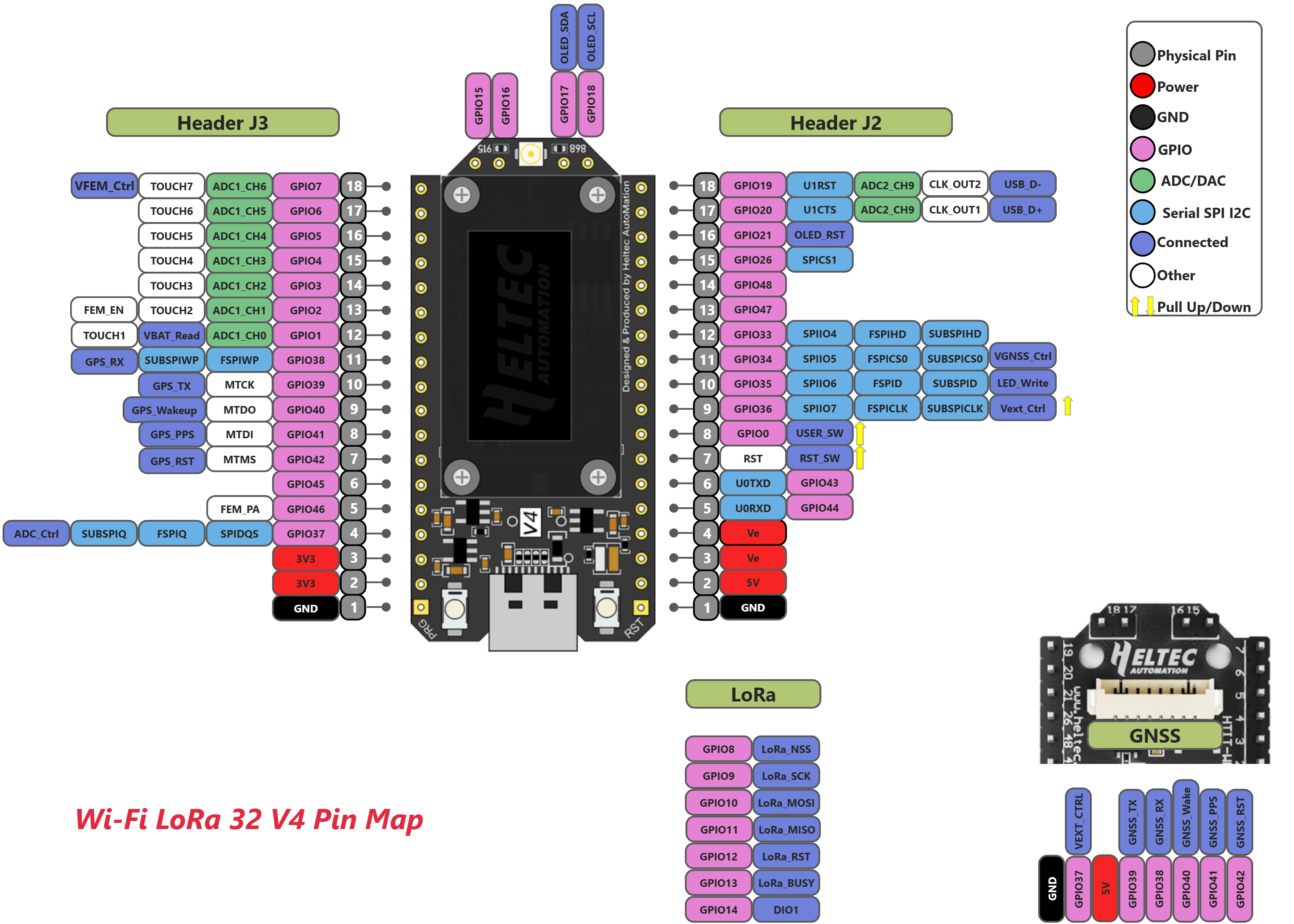
While the V4 board is also [claimed to be] pin-compatible with the V3 boards, it includes four additional pins on one end of the board and additional 2P and 8P JST connectors explicitly identified for connection to a solar panel and GNSS receiver respectively. Two of those additional pins now provide access to the I2C bus used for the onboard OLED display (see comment on I2C bus usage above).
Additional Components
There are also some additional components in the LoRa circuitry, in particular the GC1109 RF power amplifier that underpins the increased power now available in the 868~928MHz frequency range. I'm not aware of a 433MHz version of the V4 board but, given that the GC1109 quite explicitly operates in the 860~930MHz band, a 433MHz version would have to include a different amplifier, or simply do without one.
Of note then is the fact that there are now several additional control functions, VFEM_Ctrl (GPIO7), FEM_EN (GPIO2) and FEM_PA (GPIO46) (FEM = Front-End Module), used in conjunction with this RF power amplifier. As such, the V4 board is not truely pin compatible with the V3 board as these three pins are now no longer available for other uses when LoRa is configured.
The same seems to apply to several other pins, although the only one I can confirm at this point is GPIO34, which is identified as being used for VGNSS_Ctrl. I thought that this would mean that GPIO34 would be available if the GNSS module was not configured but this does not appear to be the case. It would appear that GPIO34 is RESERVED for this function—I was unable to successfully configure a OneWire bus on GPIO34. I am yet to confirm whether or not GPIO38~GPIO42 might have suffered a similar fate, also being allocated for functions associated with the [optional] GPS module.
In the present context it is also important to appreciate that, while the operation of the RF power amplifier is implicitly managed when using the Heltec LoRaWan_APP library, it must be explicitly managed when using other LoRa/LoRaWAN libraries, such as the RadioLib library. The following then is an example of the code elements required to activate the power amplifier on the V4 board, now a necessary precursor to the effective use of the LoRa radio, and initialise LoRa using the RadioLib library.
|
Refer to the LoRa Configuration page for more detail.
No UART
The V4 board does away with the Silicon Labs CP2102 USB to UART bridge found on earlier board revisions. Instead, it uses the USB Communications Device Class, or USB CDC, a component of the core software that can be used in place of a hardware UART or the like to communicate directly between the USB interface and the ESP32 SoC.
The critical issue here is that there is now an option available in the IDE Tools menu to enable or disable USB CDC On Boot. This parameter must be enabled for the V4 board to use the IDE Serial Monitor for Serial output. The default setting is specified in the ~/Documents/Arduino/hardware/heltec/esp32/boards.txt file and, at the time of writing, was Disabled, requiring USB CDC On Boot to be explicitly Enabled through the IDE Tools menu prior to uploading any code to the processor if output to the Serial Monitor is required. In reality, for compatibility with the characteristics of previous board versions if nothing else, the relevant entries in the boards.txt file should read as follows:
|
5 Nov 25 This change has now been made in the master available from the WiFi_Kit_series GitHub repo (which, for reasons best known to Heltec, is not actually accessible through the main Heltec GitHub site).
Another consequence of this change would appear to be that GPIO19 and GPIO20 are no longer generally available as they are used by the internal USB CDC. Why GPIO19 and GPIO20, labelled for the second UART (U1) on the pin map, rather than GPIO43 and GPIO44, which are labelled for the first UART (U0) on the pin map, I am yet to discover. There's a bit more testing to do here but, at the moment, it does not appear that GPIO19 and GPIO20 can be used generally as GPIOs as they previously were. Either way, the pin map is not entirely accurate with regard to the labels on the relevant pins as there are no UARTs at all on the V4 module.
Serial communications used when uploading code are not controlled by this setting.
Refer to the Espressif documentation for more details on the options that can be configured through the Arduino Tools Menu and the subject of USB CDC and DFU Flashing.
Vext Control
While there is no indication in the board schematic of any change in the circuitry, Vext control is back to the way is was prior to the release of the V3.2 board. To turn Vext power ON, set Vext LOW and to turn it OFF, set Vext HIGH.
The upshot of this is that the V3.2 board is a complete aberration in relation to Vext control and a thorough pain when it comes to software compatibility between WiFI LoRa 32 board hardware revisions. Fortunately for me, I have never built any software around a V3.2 board, but this also means that no WiFi LoRa 32 code on this site that uses Vext will work as intended on a V3.2 board without changing the Vext control logic.
OLED Display
While the V4 board uses an SSD1315 OLED display, it would appear to be software compatible with the SSD1306 displays used on previous board revisions to the extent that I have not needed to change the display library in any of my applications.
It seems that there is also a version of the V4 board that is supplied without an onboard display but which can be connected to an external display, a larger one, or maybe an e-paper display, for example, through the same connector. Unfortunately, while the connector appears to be of a type that is quite commonly used in the internals of electronic devices, it is not a standard header or JST type of connector so it's not obvious yet how useful/practical this feature will be.
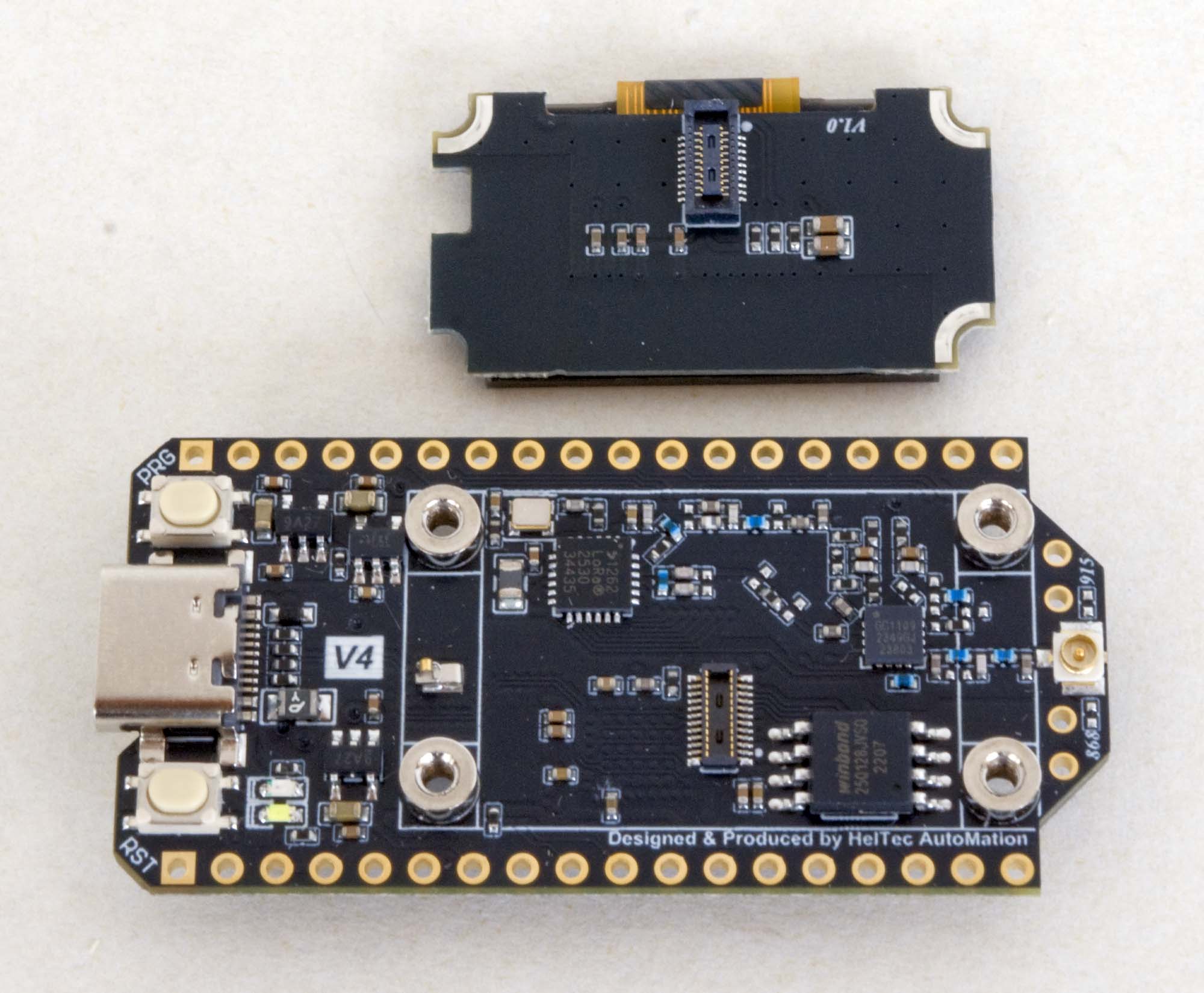
Display Connector
The onboard WiFi antenna is located around the top left corner of the OLED display cover, connecting to the motherboard through a spring-loaded contact. It's not clear what implications this might have for a board without the standard display, but maybe that's also why there's an IPEX WiFi antenna connector on the back of the V4 board.
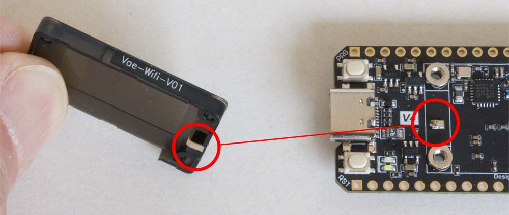
WiFi LoRa 32 V4 WiFi Antenna
The location of this antenna seems also to have necessitated the use of a plastic screw in the top left corner of the cover, rather than the metal screws used on the other three corners. It might have been smarter to simply use plastic screws all round, although the head of the plastic screw on one of the modules I received was quite badly damaged, presumably through an attempt to tighten it with the same [unnecessarily high] tension used on the metal screws.
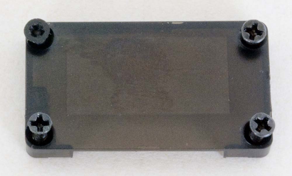
Display Cover Screw Head Damage
Heltec WiFi LoRa 32 (V4.3.1)
The V4.3.1 board (click here to view the schematic) is an update of the V4.2 board. Frustratingly, Heltec have once again arbitrarily changed the function of some of the GPIO pins, in this case GPIO5 and GPIO46. On the V4.2 board, GPIO46 was assigned to the FEM_PA function and GPIO5 was available for general use. GPIO5 now appears to have been assigned to the FEM_PA function and, while not entirely clear, it appears that GPIO46 is now available for general use. The frustrating part here is that the changes appear quite arbitrary. One can only assume that the change has been made based on convenience in the board layout rather than any higher level logic.
I do not have one of these boards yet so it is difficult to offer any further comment at this point.
Heltec Wireless Stick Lite
The Wireless Stick Lite (Panda Board) pin functions are presented in the following pinout diagram. Note once again that the Heltec boards do not use the ESP32-WROOM-32 processor module. As such, there are some GPIOs available on these boards, notably GPIO37 and GPIO38, that are not broken out on the ESP32-WROOM-32 or boards based on that processor module.
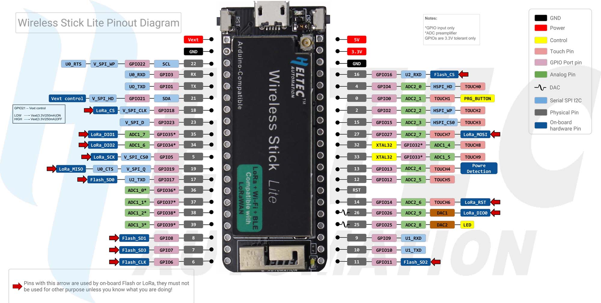
1 2 3 4 5 6 7 8 9 10 11 12 13 14 15 16 17 18 19 20 21 22 23 24 25 26 27 28 29 30 31 32 33 34 35 36 37 38 39 40 41 42 43 44 45 46 47 48 49 50 51 52 53 54 |
#define Builtin_LED25
#define GPIO00 #define GPIO11 #define GPIO22 #define GPIO33 #define GPIO44 #define GPIO55 #define GPIO66 #define GPIO77 #define GPIO88 #define GPIO99 #define GPIO1010 #define GPIO1111 #define GPIO1212 #define GPIO1313 #define GPIO1414 #define GPIO1515 #define GPIO1616 #define GPIO1717 #define GPIO1818 #define GPIO1919 #define GPIO2121 #define GPIO2222 #define GPIO2323 #define GPIO2525 #define GPIO2626 #define GPIO2727 #define GPIO3232 #define GPIO3333 #define GPIO3434 #define GPIO3535 #define GPIO3636 #define GPIO3737 #define GPIO3838 #define GPIO3939 #define TXGPIO1 #define RXGPIO3 // SPI (LoRa) #define SCKGPIO5 #define MISOGPIO19 #define MOSIGPIO27 #define CSGPIO18 #define NSSGPIO18 #define RSTGPIO14 #define DIO0GPIO26 #define IRQGPIO26 #define DIO1GPIO35 #define DIO2GPIO34 |
Heltec Wireless Stick Lite (V2.1)
It was recently brought to my attention that there was at least a V2.1 of the Wireless Stick Lite board. I had hitherto never heard of any V2 board, nor seen any documentation that suggested that such a board might differ in any way from the original board described above. Nonetheless, if there appear to be anomalies when using a V2 or V2.1 board, it might be worth looking at the differences between the various revisions of the WiFi LoRa 32 board described above.
Heltec Wireless Stick Lite (V3)
Like the WiFi LoRa 32 (V3) dev-board, the Wireless Stick Lite (V3) employs the ESP32-S3 processor, the SX1262 LoRa node IC and has a completely different pin configuration to the previous versions. As a result, like the WiFi LoRa 32 (V3) dev-board, it is largely incompatible with anything designed for earlier versions of this board.
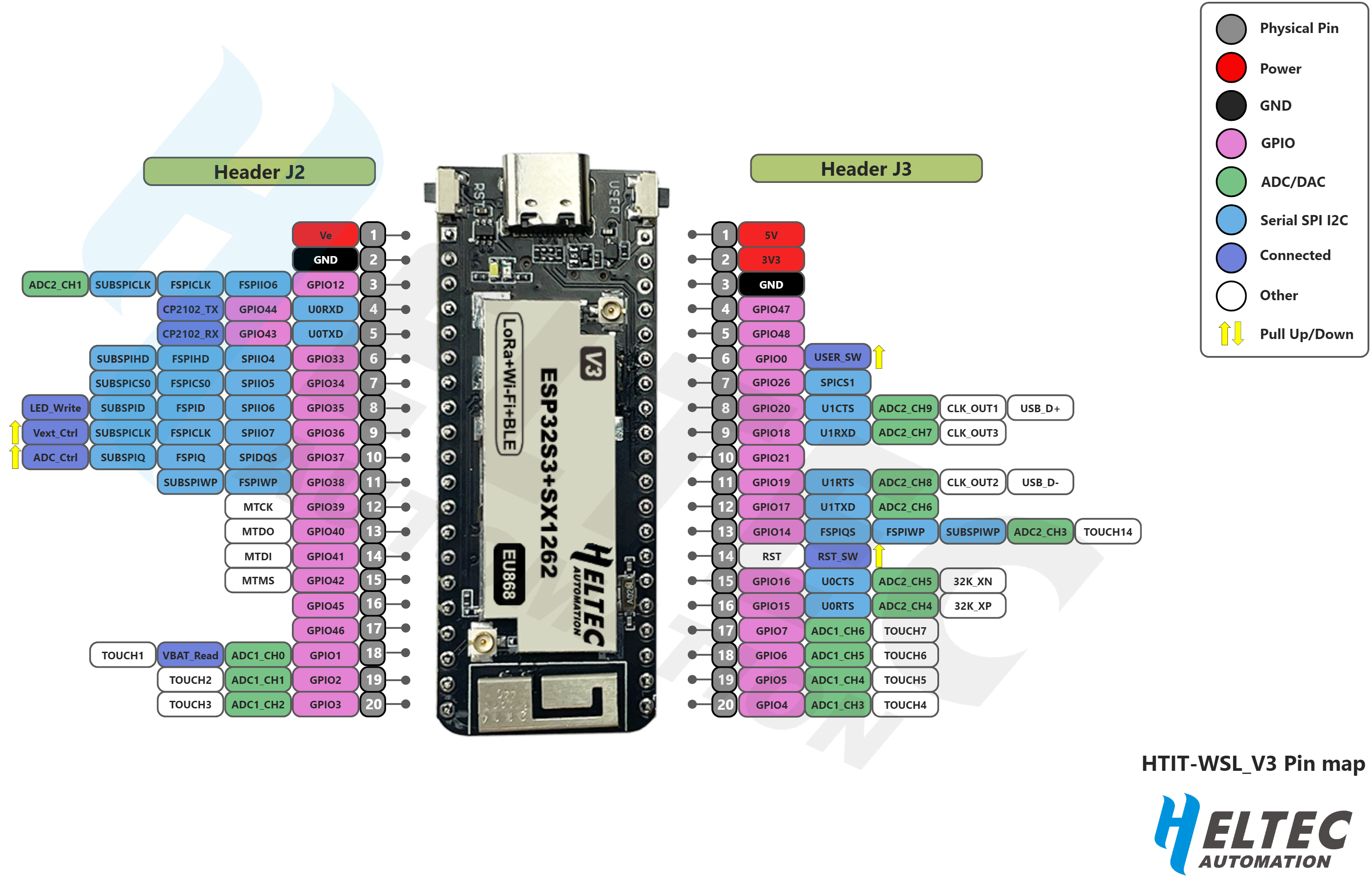
The pin configuration, used in my applications for this board, is as closely aligned with that of the WiFi LoRa 32 V3 as was practical. In the present case, there are six more GPIO pins available for general use, due to the larger pin headers (2×20 vs 2×18) and the absence of a built-in OLED display. I could not easily make all of these pins available on the baseboard I have designed, but the option is always there to expand the configuration in the future. In most cases, this will simply involve the incorporation of an appropriate header or JST connector to provide connectivity to an auxiliary board where these connections can be utilised.
1 2 3 4 5 6 7 8 9 10 11 12 13 14 15 16 17 18 19 20 21 22 23 24 25 26 27 28 29 30 31 32 33 34 35 36 37 38 39 40 41 42 43 44 45 46 47 48 49 50 51 52 53 54 55 56 57 58 59 60 61 62 63 64 65 66 67 68 69 70 71 72 73 74 75 76 77 78 79 80 |
// Most pins on the Wireless Stick Lite V3 module are
// physically numbered according to their logical pin // number #define Builtin_LED35 #define GPIO00 #define GPIO11 #define GPIO22 #define GPIO33 #define GPIO44 #define GPIO55 #define GPIO66 #define GPIO77 #define GPIO1010 #define GPIO1111 #define GPIO1212 #define GPIO1313 #define GPIO1414 #define GPIO1515 #define GPIO1616 #define GPIO1717 #define GPIO1818 #define GPIO1919 #define GPIO2020 #define GPIO2121 #define GPIO2626 #define GPIO3333 #define GPIO3434 #define GPIO3535 #define GPIO3636 #define GPIO3737 #define GPIO3838 #define GPIO3939 #define GPIO4040 #define GPIO4141 #define GPIO4242 #define GPIO4343 #define GPIO4444 #define GPIO4545 #define GPIO4646 #define GPIO4747 #define GPIO4848 // General #define USR_ButtonGPIO0 #define VBAT_ReadGPIO1 #define LED_WriteGPIO35 #define Vext_CtrlGPIO36 #define ADC_CtrlGPIO37 #define TXGPIO43 #define RXGPIO44 // I2C #define SDAGPIO19 #define SCLGPIO20 // LoRa SPI #define CSGPIO8 #define NSSGPIO8 #define MOSIGPIO10 #define MISOGPIO11 #define SCKGPIO9 #define RSTGPIO12 #define DIO0GPIO26// This may not be correct... #define DIO1GPIO14 // ALF4all #define A4a-A0GPIO2 #define A4a-A1GPIO6 #define A4a-A2GPIO33 #define A4a-A3GPIO40 // Wind/Rain #define rainCollectorPinGPIO34 #define windDirectionPinGPIO47 #define windSpeedPinGPIO48 |
LoRa MAC Address
To derive a four byte MAC address for the ESP32 processors that are used in my network, all of which include WiFi, I have used my local prefix of 0xDC followed by the last three bytes of the WiFi MAC address.
It is acknowledged that this will not result in a globally unique MAC Address, but it has, to date, served its purpose in the present environment.
Processor Interrupts
The Interrupt Service Routine (ISR) should run in RAM and not call functions that are not in RAM (Serial.X, LoRa.X etc.). In general, the ISR should only perform trivial tasks, like setting a flag or incrementing a counter. It should then be up to the main process to act on whatever the trigger might be.
My earliest attempts to write an ISR for the ESP32, which included all manner of function calls, resulted in constant processor reboots when the interrupt was triggered. The CubeCell platform seems to be a little more tolerant in this regard.
Further details pending
Processor Sleep Modes
Details pending
Asynchronous Timers
Timers are supported on the Espressif [ESP8266 & ESP32] platforms through the Ticker.h library, available through the Library Manager within the Arduino IDE.
Several implementations of the Ticker library are available. I generally use the Bert Melis version. While the Stefan Staub version uses a slightly different call structure, it could also easily be adapted for use in the present environment.
Further details pending
Analog-to-Digital Converter (ADC) Usage
The ESP32 processor includes two, 12-bit (0..4095), 3.3V analog-to-digital converters (ADCs). On the ESP32-D0WDQ6 MCU (Heltec pre-V3 boards), eight GPIOs are multiplexed into the first ADC and 10 into the second, as noted in the following table.
ESP32-D0WDQ6 ADC Configurations
| ADC1 | |
|---|---|
| Mux Port | GPIO |
| ADC1_0 | 36 |
| ADC1_1 | 37 |
| ADC1_2 | 38 |
| ADC1_3 | 39 |
| ADC1_4 | 32 |
| ADC1_5 | 33 |
| ADC1_6 | 34 |
| ADC1_7 | 35 |
| ADC2 | |
|---|---|
| Mux Port | GPIO |
| ADC2_0 | 4 |
| ADC2_1 | 0 |
| ADC2_2 | 2 |
| ADC2_3 | 15 |
| ADC2_4 | 12 |
| ADC2_5 | 13 |
| ADC2_6 | 14 |
| ADC2_7 | 27 |
| ADC2_8 | 25 |
| ADC2_9 | 26 |
In practice, however, there are caveats on the use of the pins coloured in pink in the above table and ADC2 is not available when WiFi is configured. Accordingly, for maximum compatibility, ADC usage on Heltec V1 and V2.x boards should generally be confined to ADC1, GPIOs 32–33 and 36–39.
On the ESP32-S3 MCU (Heltec V3 boards), ten GPIOs are multiplexed into each ADC, as noted in the following table.
ESP32-S3 ADC Configurations
| ADC1 | |
|---|---|
| Mux Port | GPIO |
| ADC1_0 | 1 |
| ADC1_1 | 2 |
| ADC1_2 | 3 |
| ADC1_3 | 4 |
| ADC1_4 | 5 |
| ADC1_5 | 6 |
| ADC1_6 | 7 |
| ADC1_7 | 8 |
| ADC1_8 | 9 |
| ADC1_9 | 10 |
| ADC2 | |
|---|---|
| Mux Port | GPIO |
| ADC2_0 | 11 |
| ADC2_1 | 12 |
| ADC2_2 | 13 |
| ADC2_3 | 14 |
| ADC2_4 | 15 |
| ADC2_5 | 16 |
| ADC2_6 | 17 |
| ADC2_7 | 18 |
| ADC2_8 | 19 |
| ADC2_9 | 20 |
The above table simply includes the data from the ESP32-S3 Series Datasheet. I am yet to actually use the ADCs on a Heltec V3 board although I note from the WiFi LoRa 32 V3 pin map that the GPIOs in pink in the above table are not broken out on this board. More of the GPIOs associated with ADC2 (12 & 14–18) are broken out on the Wireless Stick Lite V3 board but, once again, I am yet to actually use the ADCs on this board and cannot comment on any usage restrictions that may exist although, once again, ADC2 is not available when using the ESP32's WiFi capabilities.
Further details pending
In the interim, see also this discussion in relation to the use of various ADCs in the measurement of battery voltage.
EEPROM Usage
14 Mar 23 Since writing this section, I have developed the EepromHandler library, which includes all of the functions required to access an I2C EEPROM in the present environment. In due course, I will move the following discussion to the section that describes the functions of the EepromHandler.
There are two issues that arise in relation to external I2C EEPROM usage.
The first is the simple fact that EEPROM size is generally specified in bits, while content is stored and retrieved in 8-bit bytes. As such, a typical 2K[bit] EEPROM is actually capable of storing only 256 bytes of data, a 4K[bit] EEPROM 512 bytes, an 8K[bit] EEPROM 1K Bytes, and so on.
The second is the mechanism used to address individual bytes in an EEPROM, which can vary with the size of the EEPROM. This caused me no end of grief early on because I had purchased an 'assortment' of EEPROMs, ranging from 2K to 64K in size, and I was using them more or less randomly in my applications without any appreciation for the fact that they may not all have been able to be used in the same way, their differing capacities notwithstanding.
Unfortunately, using the simple addressing mechanism described below doesn't just restrict a larger EEPROM to 16K[bits], it simply doesn't work—at least, it didn't work for me.
2K – 16K EEPROMs
A number stored in a single 8-bit byte provides the ability to address 256 discrete locations. Atmel/Microchip AT24Cxx EEPROMs also include 3 bits of hardware-level addressing. This latter feature allows up to eight EEPROMs to reside on a single I2C bus, but conditions apply—the total addressable content is still only 8 × 256 = 2K bytes. A 16K EEPROM (16Kbits = 2KBytes) alone, for example, thus requires all of this addressing capability. However the 16K[bits] of EEPROM is configured, as a single 16K EEPROM or as several smaller EEPROMs (with appropriate Vcc or GND connection of their A0..A2 pins to set the relevant 3-bit hardware address), it is accessed in 256 byte blocks, via individual I2C addresses—0x50..0x57.
The Serial Monitor output from the Louis Llamas I2CScanner example sketch (Arduino I2CScanner library), run on an ESP32 processor (A4a‑ESP32‑WROOM‑32) connected to a 16K EEPROM (I2C addresses 0x50..0x57) and a BME280 sensor (I2C address 0x76) helps to illustrate the situation:
18:42:07.344 -> --- Scan started ---
18:42:07.381 -> I2C device found at address 0x50  !
18:42:07.381 -> I2C device found at address 0x51  !
18:42:07.381 -> I2C device found at address 0x52  !
18:42:07.381 -> I2C device found at address 0x53  !
18:42:07.381 -> I2C device found at address 0x54  !
18:42:07.381 -> I2C device found at address 0x55  !
18:42:07.381 -> I2C device found at address 0x56  !
18:42:07.381 -> I2C device found at address 0x57  !
18:42:07.381 -> I2C device found at address 0x76  !
18:42:07.381 -> --- Scan finished ---
In this case, to set the internal EEPROM address from which to read, or to which to write, we first nominate an appropriate I2C address, then send the single byte address of the relevant location within that memory block:
|
All of the applications described on this site currently use only I2C address 0x50 for EEPROM access and, as such, only ever use the first 2K of any [2K – 16K] EEPROM.
Some applications, however, assume that a 32K or 64K EEPROM is configured and use the extended addressing mechanism described below. These applications still only access I2C address 0x50, but in this case they have access to 32K[bits] of EEPROM storage. Where this is relevant, it is explicitly noted.
Refer to the relevant Atmel AT24Cxx or AT24C16C, or Microchip AT24Cxx or AT24C16D datasheets for more information.
See also this project on the Arduino Project Hub.
32K & 64K EEPROMs
The 32K EEPROM uses I2C address 0x50 and the 64K EEPROM uses addresses 0x50 and 0x51 to access 32Kbit (4KByte) blocks of storage. A two-byte software addressing mechanism must then be used to access individual locations within these blocks.
In this case, to set the internal EEPROM address from which to read, or to which to write, we first nominate an appropriate I2C address, then send the internal address in two bytes as follows:
|
The above process effectively masks the upper and lower 8-bit bytes of the address and sends them, Most Significant Byte (MSB) first, to the device. Most examples specify the address variable as a long integer (long int or just long), even though most 'Arduino' processors use 32 bits for a long integer and 16 bits, which is all we need, for an int. Regardless, the process illustrated above extracts the 'lower' 16 bits from the relevant variable.
Note that this mechanism does not yield the same result as would the simple mechanism previously illustrated, if used on a smaller capacity EEPROM that only requires an address that occupies a single byte. In such a case, the first byte of the 2-byte address that is sent will always be zero and the full address will be contained in the second byte. In the case of the single byte address, the address is contained in the first and only byte.
If a 2-byte address is sent to a device expecting a single byte address, the first byte will be accepted as the address, but the second byte will then be assumed to be the first byte of data that is to be written to the address specified by the first byte—usually zero in such a case but, whatever it is, anything at that location will then be overwritten—even if the actual intent was only to read from the EEPROM.
Refer to the Atmel AT24C32/64 datasheet for more information.
128K, 256K and 512K EEPROMs
The two-byte addressing mechanism must also be used with 128K, 256K and 512K EEPROMs, although in these cases memory is accessed in blocks of 64Kbits, for the 128 & 256K EEPROMs, or 128Kbits for the 512K EEPROM. I have not, however, used any of these devices.
Refer to the Atmel AT24C128/256 and AT24C512 datasheets for more information.
This Microchip Application Note outlines a means by which the required addressing mechanism for individual EEPROMs can be determined dynamically. A class method based on this mechanism is provided in the EepromHandler library discussed elsewhere on this site.
EEPROM Utility
The sketch, and support files, that can be downloaded by clicking on the link below is a utility developed to reset the contents of EEPROMs used in the present environment. It includes conditional compilation directives to allow the generation of binaries suitable for ATmega328, ESP8266, ESP32 and Heltec CubeCell [Plus] platforms. The .zip archive includes pin definition files for all of the platforms described on this site (at the time of preparation) and a file that defines the EEPROM locations that can be read or written.

|
ResetEEPROM | [14 KB] |
The operation of the sketch should be self-explanatory. The EEPROM need only to be connected to the I2C pins of the relevant hardware platform, and the sketch compiled and loaded. By default, 2-byte data elements are stored at and retrieved from byte locations 0, 4 & 8 of the EEPROM at I2C address 0x50, using either Standard [1-byte] or Smart [2-byte] addressing (user selectable). The locations and data element sizes can, nonetheless, be adjusted to suit any application. Relevant commands are entered through, and results displayed in the Serial Monitor.
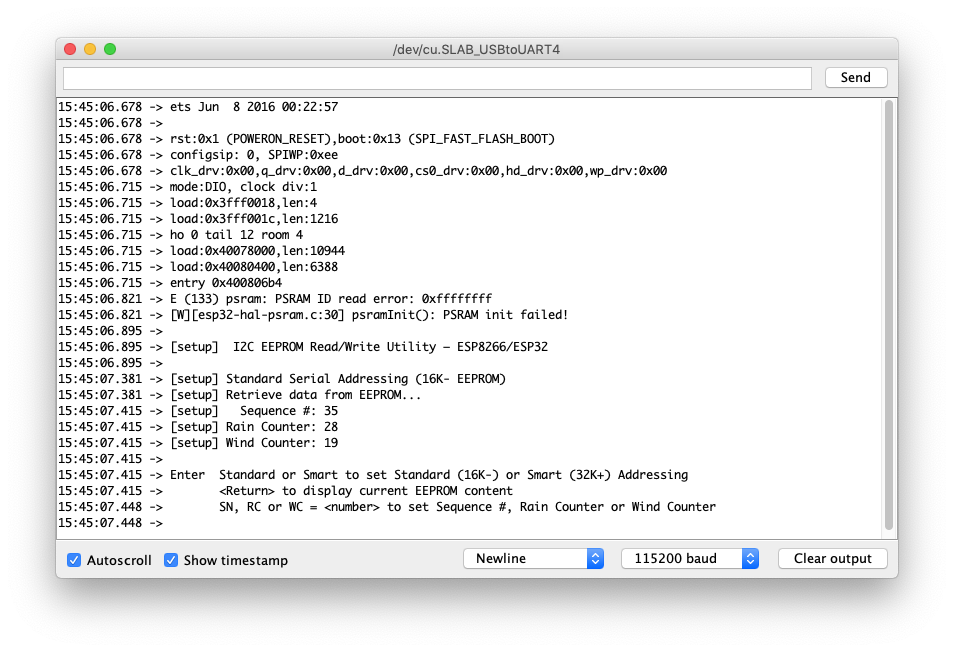
ResetEEPROM Serial Monitor Output
An updated and extended version of this utility, which uses the EepromHandler library rather than the help files used in the above version, is available from the EepromHandler Downloads page.