

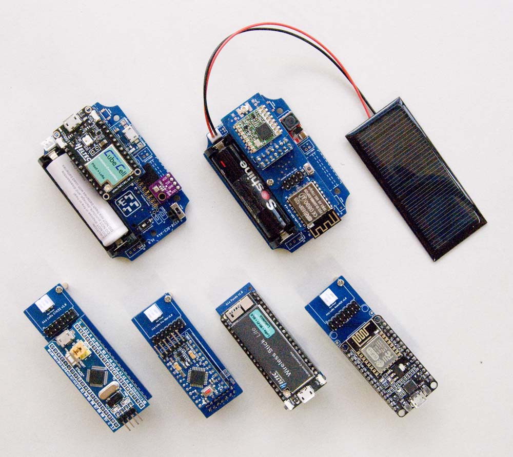
IoT Nodes
ALF4all 'Sandwich' Solar Power PCB
Unfortunately, the direct links to pages within Wijnand Nijs' ALF4all website, referred to below, no longer work as intended—they only lead to a home page and the reader must navigate through the site to find relevant information.
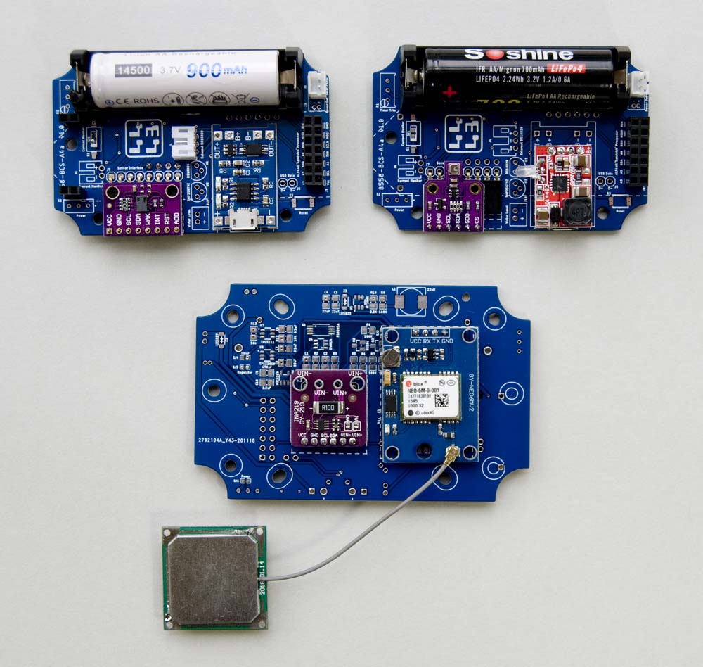
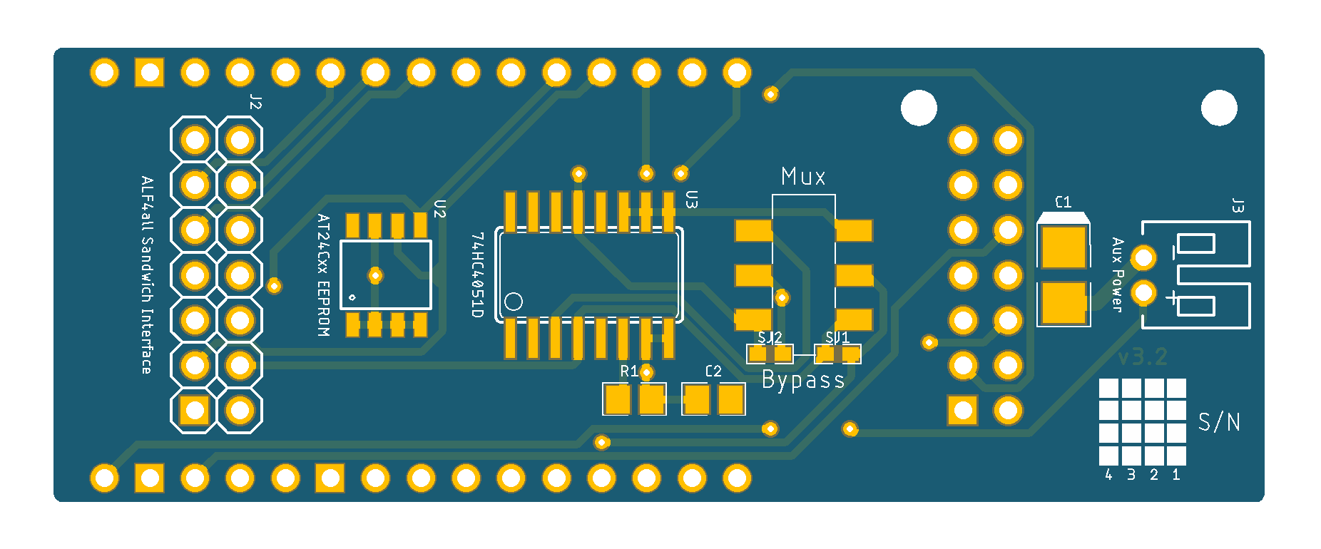
My primary prototyping board variant—in two sizes, for 85mmx58mm and 100mmx68mm enclosures respectively—is designed specifically to support the ALF4all 'Sandwich' concept processor boards originally developed by Wijnand Nijs and, as such, the ALF4all processor boards also described below. It is essentially a variant of his IoT Charger/Sensor board that has been extended to support a LiPo, Li Ion or LiFePO4 battery and an appropriate charging module with solar panel input.
The boards support a range of sensors including:
- TMP35/TMP36 (temperature)
- DS18B20 (temperature)
- BMP180 (temperature, pressure)
- BMP280 (temperature, pressure)
- BME280 (temperature, pressure, humidity)
- BME680 (temperature, pressure, humidity, gas)
- MAX44009 (ambient light)
- CCS811 (VOX)
- VEML6075 (UVA, UVB, UVI)
- NEO-6M (GPS)
The current board can also be configured with the following sensors:
- Davis 6466M (rainfall)
- Davis 6410 (wind speed)
- Davis 6410 (wind direction)
- HDL300 (water pressure/depth)
- MPS20N0040D ([line] air pressure)
- AJ-SR04M (ultrasonic distance)
- YF-G1 (water flow)
- Pressure Transducer ([line] water pressure)
As such, with the appropriate software configuration, the boards should support any sensor with a physically compatible I2C interface. Many weather sensors also use RJ11 connectors that are compatible with the Davis units listed above so, once again, with an appropriate software configuration any compatible weather sensors should also be supported. And finally, any two-wire sensor that provides a simple variable current or voltage output, operating between 3–28V (with appropriate boost converter configruation) should also be able to be connected through the 2-wire JST connector provided to support the HDL300 liquid pressure sensor.
Additional Features
To this basic concept, I have added optional support for a TP5000 battery charger module to, in turn, support the use of LiFePO4 battery technology, associated battery protection circuitry and a micro-USB connector for charging power input. I have also provided support for solar panel charging using either the TP4056 or TP5000 charging system.
I'm still working through a number of solar panels to find the smallest practical package for my application but, while I concede that it is summer here in Australia, to date even the smallest panels I've tried (80 x 35, 5.5V, 70mA) paired with a 14500 (AA) Li-Ion or LiFePO4 battery keep the battery at full charge while sending messages every 60 seconds. I have since tried a 40mA panel and it appeared to be too small to maintain the charge in the battery on the CubeCell configurations I tested. I don't really understand this observation, as the 70mA panel recharges a depleted battery in no time at all, so I will revisit this when time permits.
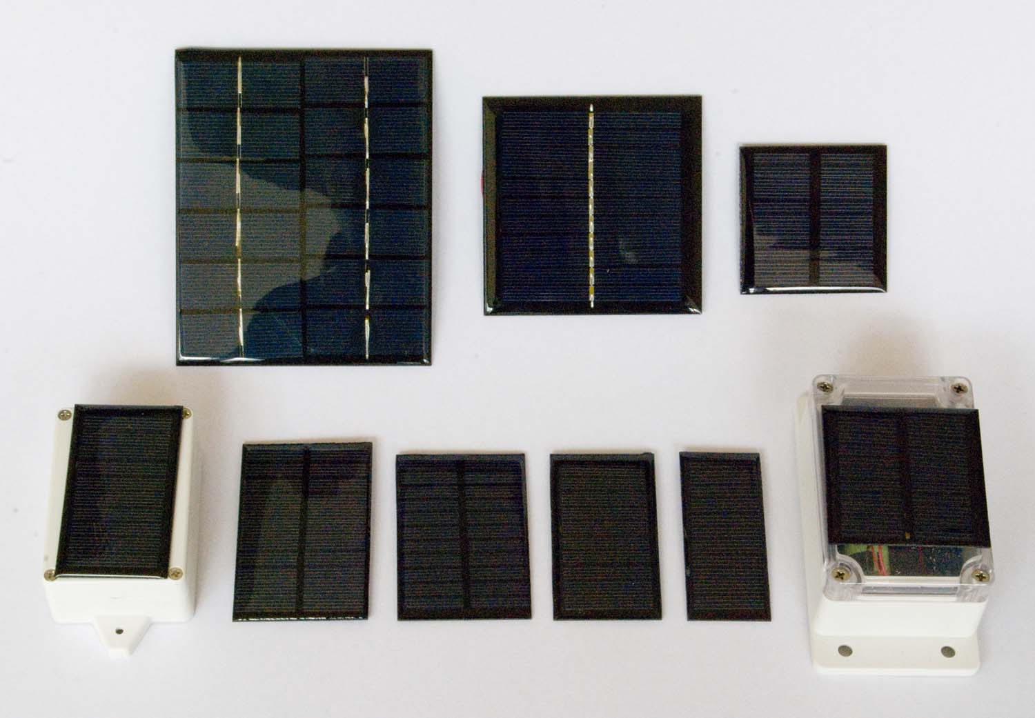
Since I live in Australia, in an area that boasts blue skies and sunshine for a significant proportion of the year, my configuration might not suit applications in other geographies. That might compromise the packaging of the overall solution, but should only require the configuration of a more appropriately sized solar panel.
As this board is intended to support Li-Ion (3.6/3.7V nominal cell voltage) batteries and 3.3V processors, it can also be configured with a 3.3V regulator. The voltage regulator can be omitted, and the associated circuitry bypassed, if this function is provided on the processor module being used or if only LiFePO4 (3.2V nominal cell voltage) batteries are used. While I've not included any specific location to physically mount a LiPo battery, a PH2.0 JST connector can be configured in place of the battery holders.
For low power applications, like the ALF4all board, it includes an optional [TPL5111/TPS22860] timer/switch circuit that can be configured to shut down the processor entirely when not in use (~1.5µA). As the shutdown time-interval is set by the value of a particular resistor, I have included options for two different styles of trimpot so that the time-interval can be adjusted manually—the physically larger trimpot provides for finer tuning of the time interval, while the physically smaller unit would provide for more compact packaging (not really an issue on this particular board).
The board also includes support for a voltage boost converter circuit to allow, in the present case, the use of a 24V water level [pressure] sensor (they're about half the price of a 5V sensor, which can run to more than $100 ea with shipping).
In addition to support for the sensors listed above, this board thus also supports:
- 18650 or 14500 format Li ion and LiFePO4 batteries
- LiPo batteries (PH2.0)
- Battery voltage monitor
- Circuit current monitor
- TP4056 or TP5000 battery managent systems, including battery protection circuitry
- Solar panel battery charging
- TPL5111 timer and TPS22860 load switch
- MIC5219 or MCP1700 voltage regulators
- 3–28V boost converter
- Configuration options selectable via solder jumper or DIP switch
Note also that this board may need to be raised slightly off the enclosure mounting pedestals (2-3mm spacers) to avoid fouling any PTH header pins adjacent to mounting points. Alternatively, the offending pins can simply be trimmed back to the level of the board.
These configuration options are described and illustrated in detail in the assembly pages.
The board design was prepared in Eagle CAD according to the following basic schematic:

Note that almost all elements in this circuit can be bypassed or omitted altogether. All that's needed in the most basic configuration is a battery [holder] and the ALF4all 'Sandwich' processor interface. Thereafter, any other features can be configured as required, to suit the application at hand.
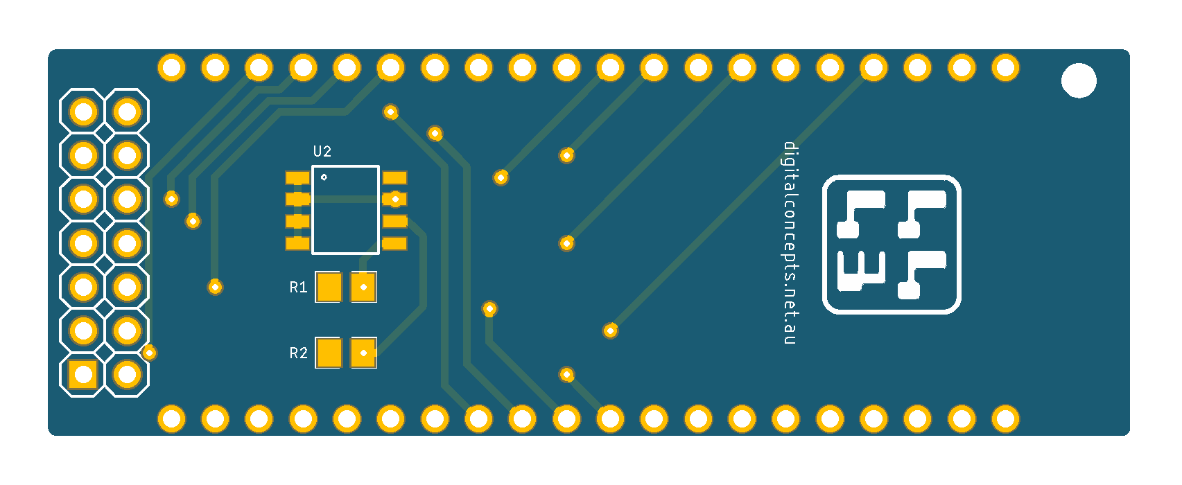
100 x 68 Enclosure (10068-BCS-A4a)
This board supports all of the features described above, including the option to configure DIP switches in place of solder jumpers to facilitate the use of different board configurations during the prototyping process.
| Top | Bottom |
|---|---|
 |
 |
10068-BCS-A4a [v4.1] PCB
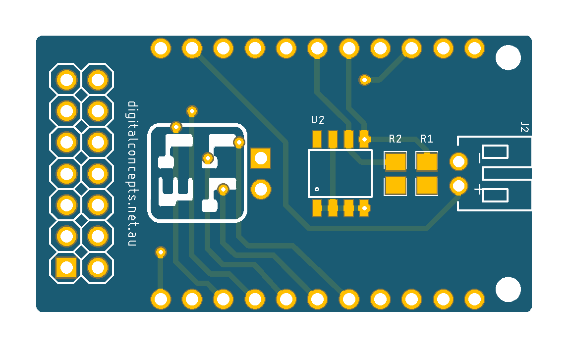
85 x 58 Enclosure (8558-BCS-A4a)
This board provides for a tighter packaging option when only a 14500 (AA) or LiPo battery is required. Not all of the above-listed features are supported, due to the size of the smaller enclosure. I'll run through all of the features that are ultimately supported when I've completed the testing process.
In reality, however, I haven't used this board much at all. Given the prototyping nature of the initial configuration of a Node, I've generally used the larger board and enclosure for prototyping work—because the DIP switches on that board are very convenient when testing different circuit elements—then just tightened up the packaging, if required, when creating a Node for a specific application.
| Top | Bottom |
|---|---|
 |
 |
8558-BCS-A4a [v2.0] PCB
ALF4all 'Sandwich' Processor PCBs
In order to test different processors with various Node configurations, I prepared a number of processor PCBs based on the Wijnand Nijs 'Sandwich' interface. These processor boards were each designed to support a specific processor, linking appropriate pins both to the 'Sandwich' interface and to my RFM9x(W) daughter board, where this latter functionality was not included with the relevant processor—the Heltec boards, for example, all include onboard SX1262 or SX1276/SX1278 [LoRa] modules.
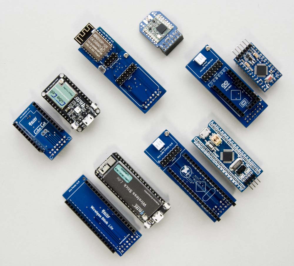
To date, I have prepared PCBs supporting the following processor modules (click on the headings to expand or the modules to zoom):
Arduino Pro Mini (+ RFM95W)
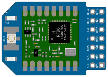
|
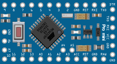
|
Includes optional support for:
- LoRa-Pi module
- EEPROM
- Auxiliary power input

A4a LoRa Pro Mini Schematic
| Top | Bottom |
|---|---|
 |
 |
A4a LoRa Pro Mini PCB

|
A4a LoRa Pro Mini Eagle CAD Files | [128 KB] |
|
|
A4a LoRa Pro Mini CAM Files | [147 KB] |
Pin Configuration
| Pro Mini | A4a Sandwich | LoRa-Pi | EEPROM | ||
|---|---|---|---|---|---|
| Pin | Pin # | Pin | Pin # | Pin | Pin |
| VCC | [1] | VCC | [8] | 3V3 | VCC |
| A3 | [2] | A3 | |||
| A5 | [3] | SCL | SCL | ||
| A2 | [4] | A2 | |||
| A1 | [5] | A1 | |||
| A4 | [6] | SDA | SDA | ||
| D9 | [7] | TxD | |||
| A0 | [8] | A0 | |||
| D13 | [9] | SCLK | [2] | SCK | |
| D8 | [10] | RxD | |||
| D11 | [11] | MOSI | [6] | MOSI | |
| D12 | [12] | MISO | [4] | MISO | |
| GND | [13] | GND | [5,11] | GND | GND, A0, A1, A2, WP |
| D7 | [14] | Ain | |||
| D6 | [1] | NSS | |||
| D2 | [3] | DIO0 | |||
| D3 | [7] | DIO1 | |||
| D4 | [9] | DIO2 | |||
| D5 | [10] | RST | |||
| [12] | DIO3 | ||||
| [13] | DIO5 | ||||
| [14] | DIO4 | ||||
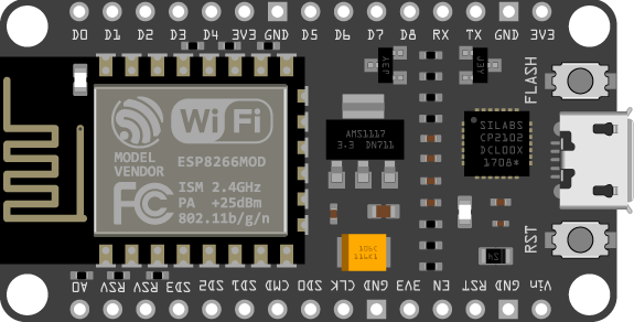
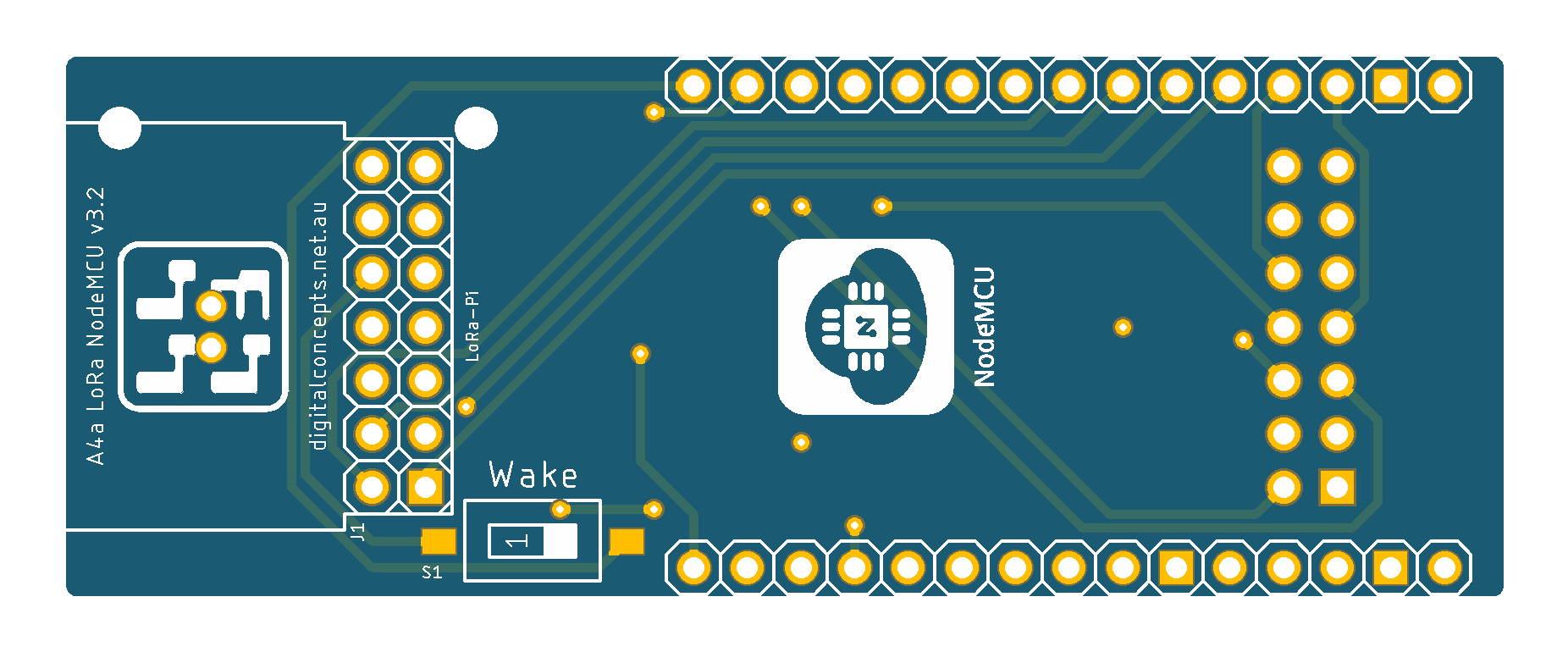
Amica ESP8266 NodeMCU (+ RFM95W)
|
|
|
See notes on pin usage under ESP-12F below.
Includes optional support for:
- LoRa-Pi module
- EEPROM
- 74HC4051 8-Channel analog multiplexer
- Auxiliary power input
- Configurable 'deep sleep' wake-reset
This board will only fit in the larger, 100 x 68 enclosure.
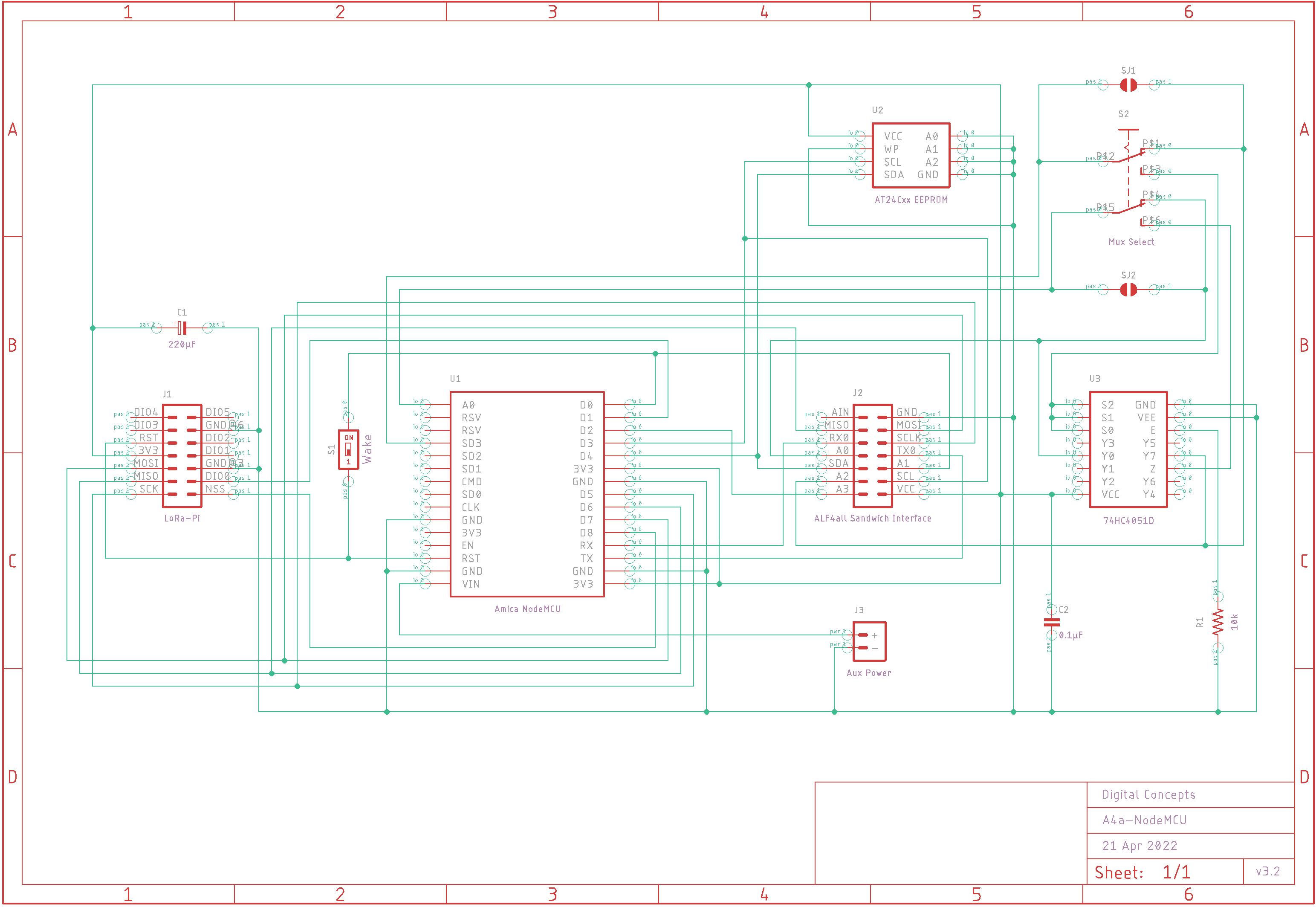
A4a LoRa NodeMCU Schematic
| Top | Bottom |
|---|---|
 |
 |
A4a LoRa NodeMCU PCB
|
|
A4a LoRa NodeMCU Eagle CAD Files | [121 KB] |
|
|
A4a LoRa NodeMCU CAM Files | [174 KB] |
Pin Configuration
| NodeMCU | A4a Sandwich | LoRa-Pi | EEPROM | Mux | ||
|---|---|---|---|---|---|---|
| Pin | Pin # | Pin | Pin # | Pin | Pin | Pin |
| VCC | [1] | VCC | [8] | 3V3 | VCC | VCC |
| D2 | [2] | A3 | ||||
| D3 | [3] | SCL | SCL | |||
| SD3 | [4] | A2 | Y7 | |||
| D0 | [5] | A1 | ||||
| D4 | [6] | SDA | SDA | |||
| TX | [7] | TxD | ||||
| A0 | [8] | A0 | Y0 | |||
| D5 | [9] | SCLK | [2] | SCK | ||
| RX | [10] | RxD | ||||
| D7 | [11] | MOSI | [6] | MOSI | ||
| D6 | [12] | MISO | [4] | MISO | ||
| GND | [13] | GND | [5,11] | GND | GND, A0, A1, A2, WP | GND |
| [14] | Ain | |||||
| D8 | [1] | NSS | ||||
| D1 | [3] | DIO0 | ||||
| [7] | DIO1 | |||||
| [9] | DIO2 | |||||
| RST | [10] | RST | ||||
| [12] | DIO3 | |||||
| [13] | DIO5 | |||||
| [14] | DIO4 | |||||
| A0 | Z | |||||
| SD3 | S0,S1,S2 | |||||
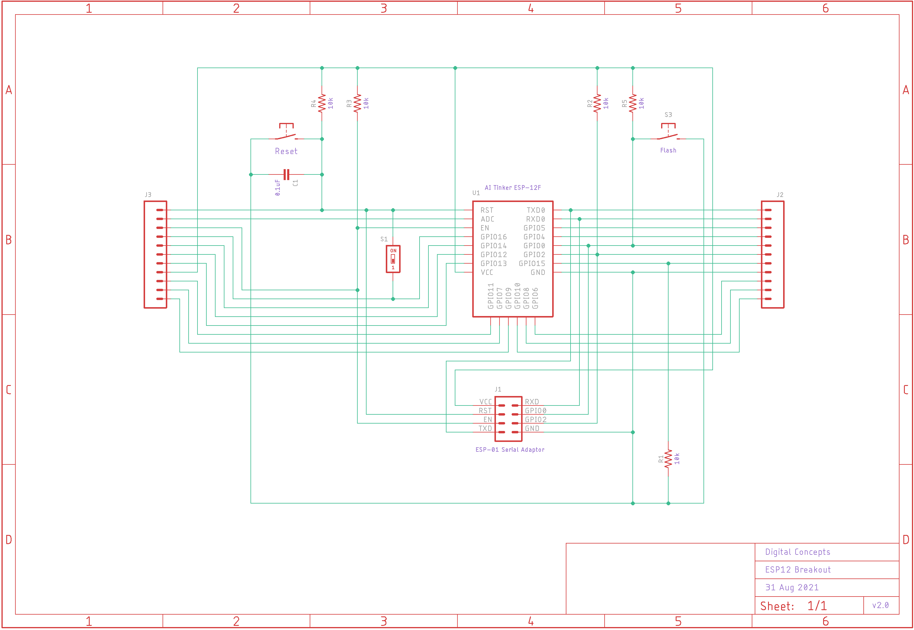
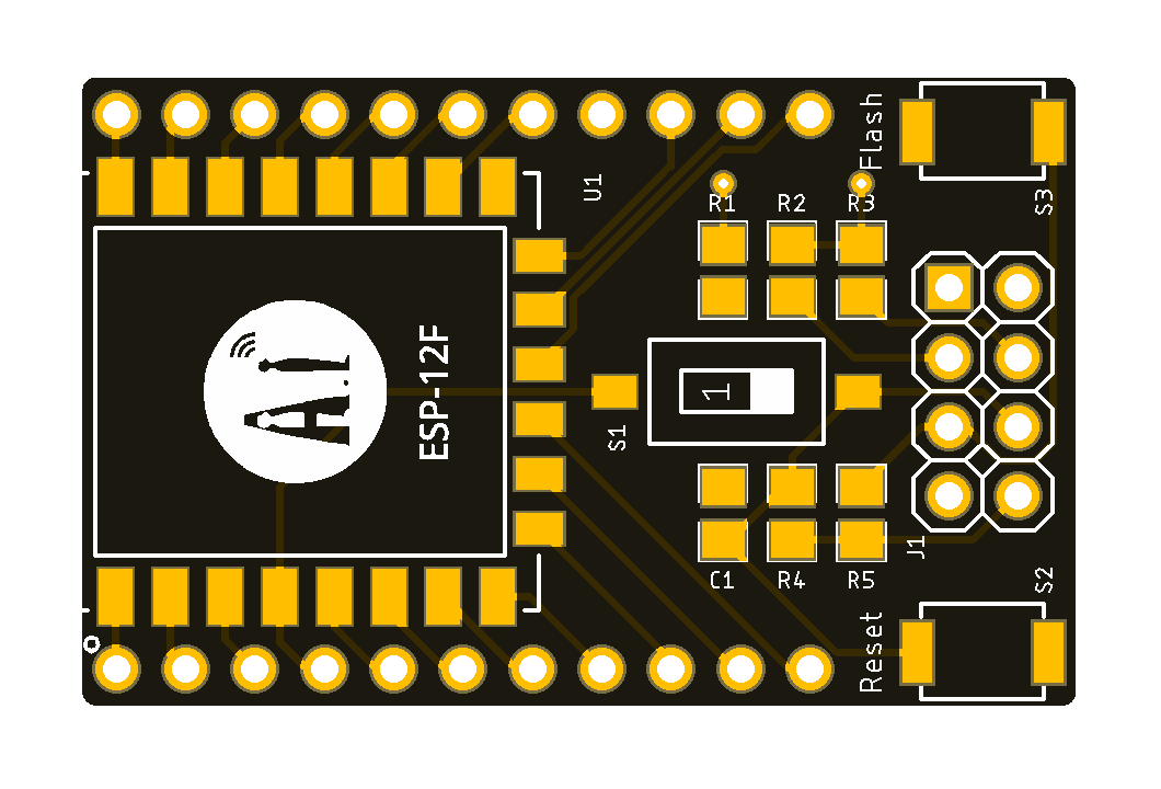
AI Thinker ESP-12F (+ RFM95W)
|
|
|
There was a bit of fiddling required to come up with a workable configuration for the ESP-12 MCU. Some pins have to be in a specific state during boot, others have reserved functions during the boot cycle or program loading, but are otherwise available, and there is only one analog channel. This article, from Random Nerd Tutorials, provides a good overview of these requirements, and this 'Instructable' provides the basic set-up/configuration instructions for the ESP12.
The first part of the pin assignment issue was resolved by using GPIO0/GPIO2 (which have specific boot and programming functions but are otherwise available) for the I2C interface, which is not used during the boot cycle or when uploading software. This freed up GPIO4 and GPIO5 (the default I2C pins) for general use, without any constraints on their boot time configurations.
The presence of only a single analog pin was resolved by adding an 8-channel multiplexer to the configuration. With GPIO4 and GPIO5 being generally used for specific functions, only one [digital] pin remained, GPIO10, which itself is only available on the ESP-12E/F modules and even then only under specific conditions. As such, with only one channel to specify a mux port, only two mux ports could be used. The 74HC4051 8-channel IC was, nonetheless, the most economical option available. This does at least allow two separate analog 'sensors' to be monitored, e.g. both analog temperature (TMP35/TMP36) and battery level, through the single ADC pin.
Unfortunately, things get even more complicated at this point. The A4a 'Sandwich' interface used for the power/sensor board supports four control channels (A0–A3), but was originally designed to support the Arduino Pro Mini, which has several pins that support both analog and digital I/O. In addition to having only a single analog input channel, the ESP-12 does not have any pins that support both analog and digital I/O.
After allocating pins for the RFM95W SPI and general I2C buses, the ESP‑12E/F has only three remaining 'free' digital pins, in addition to the single analog channel. As such, there are two possible configuration options: three digital channels and one analog channel (without using the mux) or two digital channels (one digital channel being required for mux port select) and two analog channels (using two ports on the mux).
Noting that much of the motivation for developing these boards is for prototyping work, I have included a switch on the board to allow the selection of either of these modes—the switch effectively manually toggles the 'Sandwich' A2 pin between digital and analog inputs. I will provide a more detailed description of how the switch is configured in the assembly instructions for this board, which I will provide just as soon as I get everything tested and working as intended.
If you're figuring, at this point, that it's hardly worth all of this trouble to use the ESP-12 processor in this environment, when there are several other alternatives described herein, you could well be right...
The present PCB includes optional support for:
- LoRa-Pi module
- EEPROM
- 74HC4051 8-Channel analog multiplexer
- Auxiliary power input with [optional] voltage regulator
- ESP-01 programmer interface
- Reset button
- Flash/Prog button
- Configurable 'deep sleep' wake-reset
- LED on GPIO16

A4a LoRa ESP-12 Schematic
| Top | Bottom |
|---|---|
 |
 |
A4a LoRa ESP-12 PCB
|
|
A4a LoRa ESP-12 Eagle CAD Files | [51 KB] |
|
|
A4a LoRa ESP-12 CAM Files | [218 KB] |
Pin Configuration
| ESP-12F | A4a Sandwich | LoRa-Pi | EEPROM | Mux | ||
|---|---|---|---|---|---|---|
| Pin | Pin # | Pin | Pin # | Pin | Pin | Pin |
| VCC | [1] | VCC | [8] | 3V3 | VCC | VCC |
| GPIO4 | [2] | A3 | ||||
| GPIO0 | [3] | SCL | SCL | |||
| GPIO10 | [4] | A2 | Y7 | |||
| GPIO16 | [5] | A1 | ||||
| GPIO2 | [6] | SDA | SDA | |||
| TXD0 | [7] | TxD | ||||
| ADC | [8] | A0 | Y0 | |||
| GPIO14 | [9] | SCLK | [2] | SCK | ||
| RXD0 | [10] | RxD | ||||
| GPIO13 | [11] | MOSI | [6] | MOSI | ||
| GPIO12 | [12] | MISO | [4] | MISO | ||
| GND | [13] | GND | [5,11] | GND | GND, A0, A1, A2, WP | GND |
| [14] | Ain | |||||
| GPIO15 | [1] | NSS | ||||
| GPIO5 | [3] | DIO0 | ||||
| [7] | DIO1 | |||||
| [9] | DIO2 | |||||
| RST | [10] | RST | ||||
| [12] | DIO3 | |||||
| [13] | DIO5 | |||||
| [14] | DIO4 | |||||
| ADC | Z | |||||
| GPIO10 | S0,S1,S2 | |||||
To help with my prototyping work, I also created a breakout board for the ESP-12 (S/E/F) MCU. The board provides direct breakout of all 22 ESP-12F pins, with support for the following options:
- ESP01 serial interface module
- Reset button
- Flash/Prog button
- Wake from deep sleep interrupt switch
- Pull-up resistors on EN, RST, GPIO0, GPIO2
- Pull-down resistor on IO15
ESP-12 Breakout Board Schematic
| Top | Bottom |
|---|---|
 |
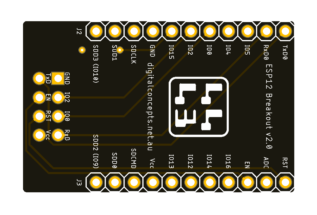 |
ESP-12 Breakout Board
After I'd done all of this, I discovered these:
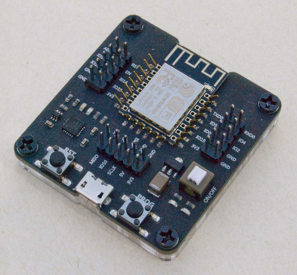
ESP-12 Programmer
available for both the ESP-12 and ESP32 processors. I now have a couple to play with and, while they're more expensive than a simple breakout board, there's no soldering required (the processor module just clips into the board—very neat!). This looks like a much more convenient way to test configurations.
Update: Having now had an opportunity to use these programmers, they're not ideal if one needs to exploit the full potential of the processor. Their hardware configuration means that not all pin configuration options are available.
In the present case, these programmers inhibit the use of GPIO0/GPIO2 for the I2C interface. Scripts seem to load OK, but something in the programmer's hardware configuration interferes with the use of at least one of these pins. Either way, scripts will not execute as intended when running on a processor within one of these programmers if the I2C interface is configured on GPIO0/GPIO2, regardless of which pin is configured as SCL or SDA.
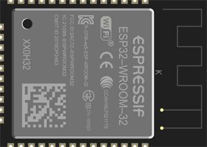
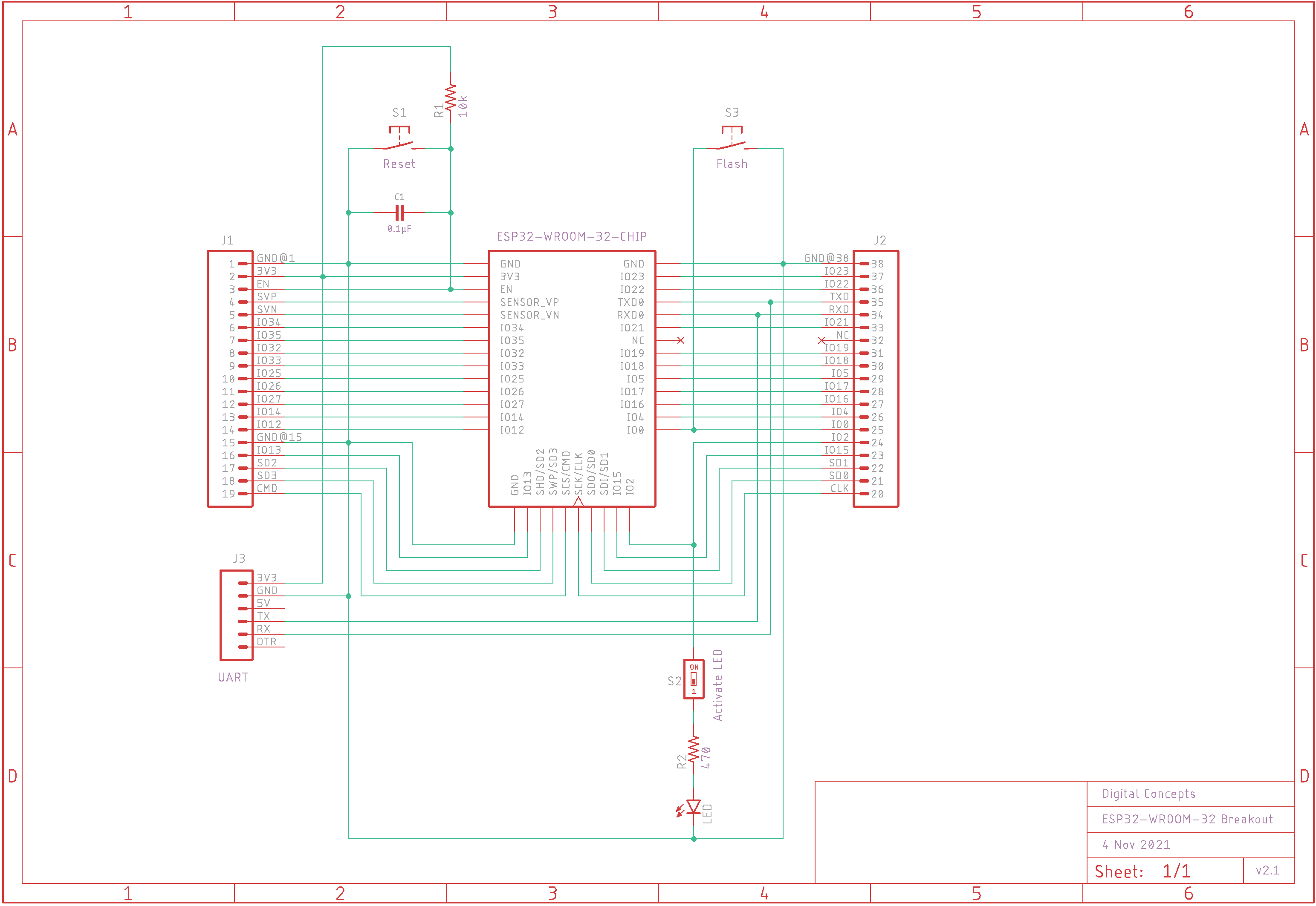
Espressif ESP32-WROOM-32 (+ RFM95W)
|
|
|
As with the ESP12 processor, the ESP32 requires certain pins to be configured or used in certain ways at certain times. Much of this is hidden from the casual user and ESP32 modules, like the ESP32-WROOM-32 used here, only break out a select subset of pins for general use. There are, however, more pins available on the ESP32 (38 on the ESP32-WROOM-32 vs 22 on the ESP-12F, although in each case some pins are reserved for specific 'system' functions) and ESP32 pin usage is generally much more flexible. The ESP32 also includes an on-board multiplexer that allows most pins to be configured, through software, for any function, including analog or digital I/O, supported by the processor.
This article, once again from Random Nerd Tutorials, provides a good overview of the ESP32 processor and associated pin usage.
The present PCB includes optional support for:
- LoRa-Pi module
- [External] EEPROM
- Auxiliary power input with [optional] voltage regulator
- USB-TTL/UART Interface
- Reset button
- Flash/Prog button

A4a LoRa ESP32 Schematic
| Top | Bottom |
|---|---|
 |
 |
A4a LoRa ESP32 PCB
|
|
A4a LoRa ESP32 Eagle CAD Files | [47 KB] |
|
|
A4a LoRa ESP32 CAM Files | [198 KB] |
Pin Configuration
| ESP32 | A4a Sandwich | LoRa-Pi | EEPROM | ||
|---|---|---|---|---|---|
| Pin | Pin # | Pin | Pin # | Pin | Pin |
| VCC | [1] | VCC | [8] | 3V3 | VCC |
| IO27 | [2] | A3 | |||
| IO22 | [3] | SCL | SCL | ||
| IO32 | [4] | A2 | |||
| IO13 | [5] | A1 | |||
| IO21 | [6] | SDA | SDA | ||
| TXD0 | [7] | TxD | |||
| IO36 | [8] | A0 | |||
| IO18 | [9] | SCLK | [2] | SCK | |
| RXD0 | [10] | RxD | |||
| IO23 | [11] | MOSI | [6] | MOSI | |
| IO19 | [12] | MISO | [4] | MISO | |
| GND | [13] | GND | [5,11] | GND | GND, A0, A1, A2, WP |
| [14] | Ain | ||||
| IO5 | [1] | NSS | |||
| IO26 | [3] | DIO0 | |||
| IO35 | [7] | DIO1 | |||
| IO34 | [9] | DIO2 | |||
| IO14 | [10] | RST | |||
| [12] | DIO3 | ||||
| [13] | DIO5 | ||||
| [14] | DIO4 | ||||
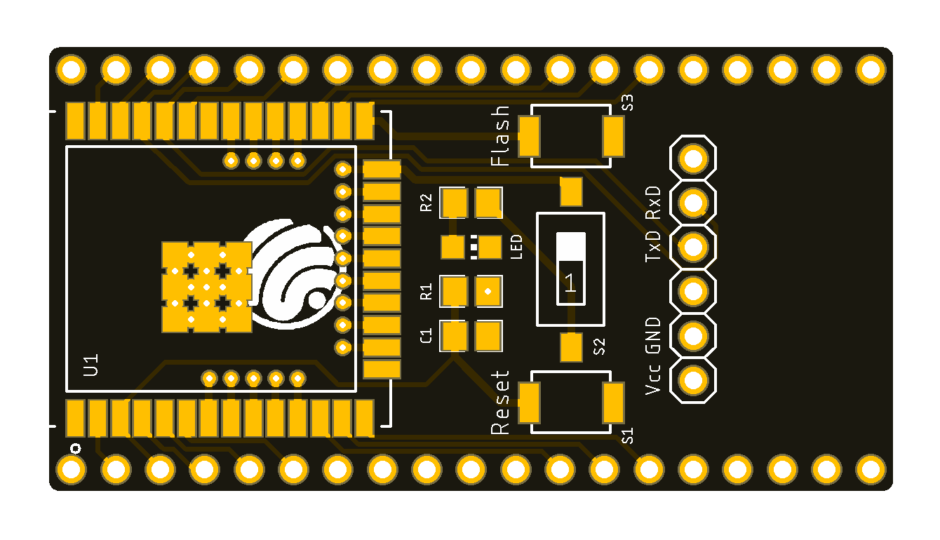
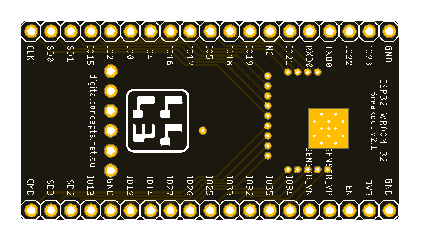
To help with my prototyping work, I also created a breakout board for the ESP32-WROOM-32 MCU. The board provides direct breakout of all 38 ESP32-WROOM-32 pins, with support for the following options:
- USB-TTL/UART Interface
- Reset button
- Flash/Prog Button
- Pull-up resistor on EN
- Switchable LED on IO2
ESP32 Breakout Board Schematic
| Top | Bottom |
|---|---|
 |
 |
ESP32 Breakout Board
For reasons I've not been able to determine, I was unable to flash the ESP32 using an ESP-01 USB to TTL adaptor (which worked fine with the ESP-12) but I had no trouble with other USB-TTL/UART modules, like this one (hence the 6-pin single row header for the USB adaptor).
After I'd done all of this, I discovered these:

ESP32 Programmer
available for both the ESP-12 and ESP32 processors. I now have a couple to play with and, while they're more expensive than a simple breakout board, there's no soldering required (the processor module just clips into the board—very neat!). This looks like a much more convenient way to test configurations. Time will tell...
STM32 (Blue Pill) (+ RFM95W)
|
|
|
Includes optional support for:
- LoRa-Pi module
- EEPROM
- Auxiliary 3.3V power input
At this point, the STM32 is a total unknown. I have a couple of modules, but I've never even loaded a sketch onto one yet, so for the time being this is little more than a thought bubble.
As a result of its physical dimensions (the board is longer and narrower than any of the others), the STM32 requires an auxiliary adaptor board to provide the ALF4all Sandwich interface and will only fit in the larger, 100 x 68 enclosure.

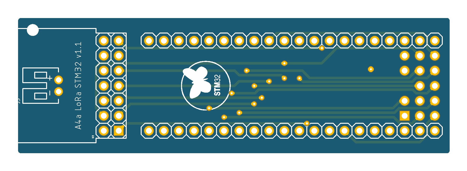
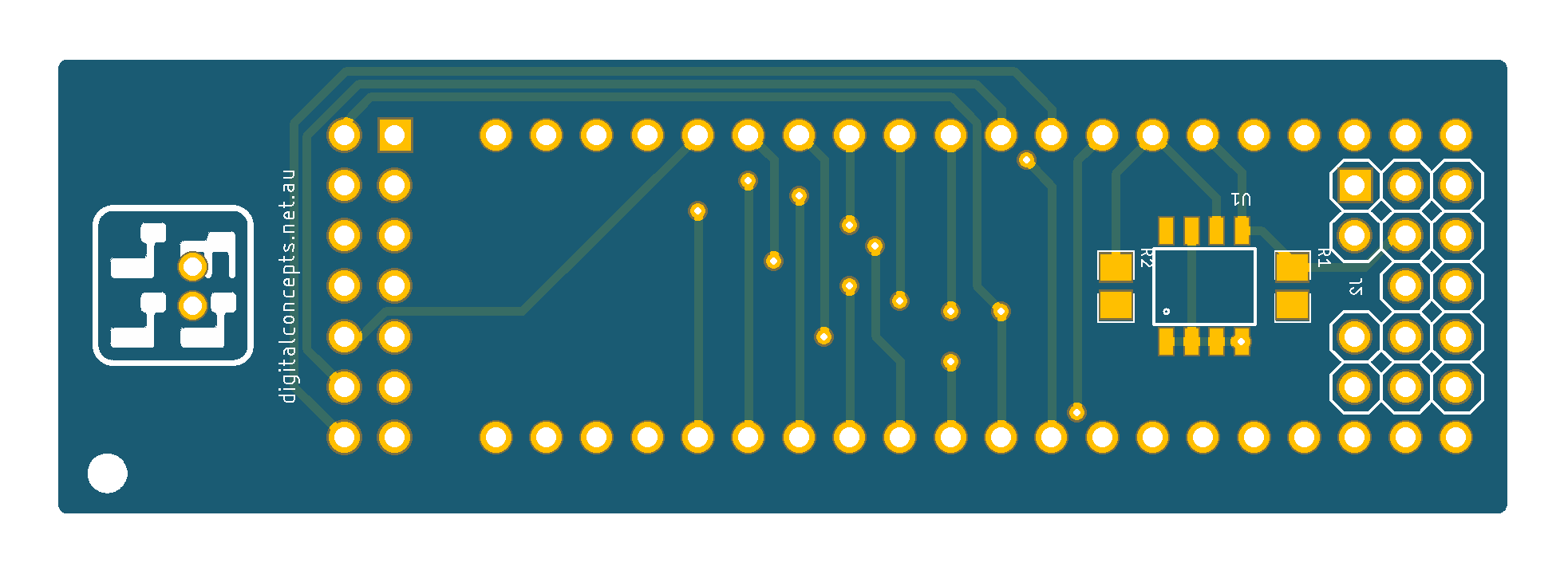
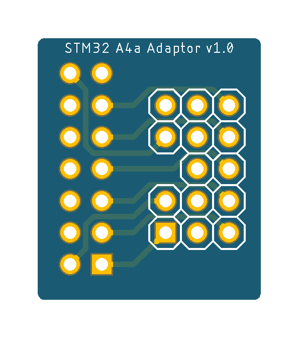
A4a LoRa STM32 Schematic
| Top | Bottom |
|---|---|
 |
 |
 |
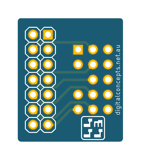 |
LoRa STM32 'Blue Pill' + A4a Adaptor PCBs
Pin Configuration
| STM32 | A4a Sandwich | LoRa-Pi | EEPROM | ||
|---|---|---|---|---|---|
| Pin | Pin # | Pin | Pin # | Pin | Pin |
| 3V3 | [1] | VCC | [8] | 3V3 | VCC |
| GPIO27 | [2] | A3 | |||
| SCL1 | [3] | SCL | SCL | ||
| GPIO26 | [4] | A2 | |||
| GPIO17 | [5] | A1 | |||
| SDA1 | [6] | SDA | SDA | ||
| TX1 | [7] | TxD | |||
| GPIO16 | [8] | A0 | |||
| SCK1 | [9] | SCLK | [2] | SCK | |
| RX1 | [10] | RxD | |||
| MOSI1 | [11] | MOSI | [6] | MOSI | |
| MISO1 | [12] | MISO | [4] | MISO | |
| GND | [13] | GND | [5,11] | GND | GND, A0, A1, A2, WP |
| [14] | Ain | ||||
| SS1 | [1] | NSS | |||
| GPIO11 | [3] | DIO0 | |||
| GPIO12 | [7] | DIO1 | |||
| GPIO15 | [9] | DIO2 | |||
| GPIO8 | [10] | RST | |||
| GPIO19 | [12] | DIO3 | |||
| GPIO21 | [13] | DIO5 | |||
| GPIO20 | [14] | DIO4 | |||
Heltec WiFi LoRa 32 (V1, V2, V2.1 & V3)
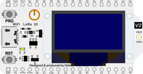
|
I did originally design an A4a processor PCB for the WiFi LoRa 32 board but, following my initial experience with the Wireless Stick Lite board (see below), I went no further. Like the other Heltec boards, the WiFi LoRa 32 board includes an on-board TP4054 charging module and, while the WiFi LoRa 32 board doesn't include a specific pin for connection to a solar panel, a solar panel can be configured as a charging source. As such, the BCS A4a base boards offer little benefit when using this and the other Heltec modules, making the development of specific battery/base boards to support the individual Heltec processor boards a more logical approach.
While I have generally tended to favour the CubeCell boards in the development of Node (as distinct from Gateway) applications to date, the Heltec WiFi LoRa 32 and Wireless Stick [Lite] development boards retain one particular advantage over the CubeCell boards: they support WiFi and bluetooth communications. As such, these boards, and the Raspberry Pi, are preferred for applications like the Gateway, that require both LoRa and WiFi/LAN communications.
The Gateway application, however, effectively needs to support the potential for continuous operation and so is not suited to support by battery alone. As such, battery power in such situations is provided more as a backup, to guarantee continued operation through power failure. The primary objective of the WiFi LoRa 32 (10068-BHWL) baseboard was therefore to provide battery backup for a primary power source in addition to the provision of a convenient mounting platform within an appropriate enclosure.
An important factor that was considered in the design of the original 10068-BHWL base board was the fact that the pin configurations of the WiFi LoRa 32 V1 & V2 boards are slightly different. The difference is mainly in the use of the various power pins but, in the present case, also impacts GPIO21. The V2 board includes a Vext pin, to control power supply to attached peripherals, and the state of this pin is controlled via GPIO21, which was previously used in the I2C interface.
This situation has been complicated even further with the release of the WiFi LoRa 32 V3 board. This board uses a different ESP32 processor (ESP32-S3FN8) and LoRa node IC (SX1262)—the ESP32-D0WDQ6 processor and SX1267 LoRa node IC had been used on earlier board revisions—and an almost entirely different pin configuration. This was way too much to attempt to accommodate on a single base board, so a new base board (10068-BHWL3) has been designed to specifically support the V3 board.
The V2 and V3 boards include on-board circuitry to monitor the battery supply voltage. There are actually two revisions of the V2 board—V2 and V2.1, although both are marked "V2" and appear identical to the casual observer—and each uses a different pin for this function. This feature was not included on the V1 board and the 10068-BHWL board includes its own battery voltage measurement circuitry. The original V2 board used GPIO13 to measure battery voltage but this apparently caused a conflict with the processor's WiFi configuration—GPIO13 used the second analog-to-digital converter, ADC2, which was not available when WiFi was configured. To address this problem, Heltec modified the V2.1 board design to use GPIO37 (an 'input only' pin) to read the battery voltage, without identifying this fact on the board hardware in any way, so it is not a simple matter to determine which configuration is applicable on any particular V2 board. This issue is discussed in detail here.
In the earlier revisions fo the 10068-BHWL board, I attempted to accommodate the differences between the V1 and V2 boards but, given that production of the V1 boards was discontinued some years ago, and even the V2 boards have now been superseded, the current revision of the 10068-BHWL board is designed for the WiFi LoRa 32 V2.1 board. It will support the earlier revisions, but possibly with limitations.
In relation to the battery monitoring circuit included on the 10068-BHWL board, a 33kΩ resistor, rather than the 27kΩ resistor used on other boards, is configured in the voltage divider to better accommodate the performance of the ESP32 ADC. While it is a 12-bit ADC (0..4095) with a voltage range of 0–3.3V, the performance of the ADC is not linear towards the ends of this range. The current voltage divider configuration thus maps the possible Li-Ion battery voltage range of 0–4.2V to a slightly reduced ADC input voltage of 0–3.16V. The difference is accounted for appropriately in software. Regardless, given that the current revisions of the WiFi LoRa 32 board include their own on-board circuitry for battery management, the 10068-BHWL battery monitoring circuitry is probably redundant and need not be configured.

| Top | Bottom |
|---|---|
 |
 |
10068-BHWL PCB
See here for CAD and CAM files.
Pin Configuration
| WiFi LoRa 32 V1/V2 | Solar Panel | EEPROM | I2C | SPI |
|---|---|---|---|---|
| Pin | Pin | Pin | Pin | Pin |
| 5V | + | |||
| 3V3/Vext | VCC | VCC | VCC | |
| GND | - | GND, A0, A1, A2, WP | GND | GND |
| OLED-SCL | SCL | SCL | ||
| OLED-SDA | SDA | SDA | ||
| LORA-SCK | SCK | |||
| LORA-MISO | MISO | |||
| LORA-MOSI | MOSI | |||
| GPIO2 | CS | |||
| WiFi LoRa 32 V1/V2 | Sensor Interface | Sensor |
|---|---|---|
| Pin | Pin | |
| 3V3 | Vcc / RST (Pull-Up) | |
| GND | GND / ADD | |
| OLED-SCL | SCL | |
| OLED-SDA | SDA | |
| GPIO23 | Sensor Wake | |
| GPIO39 | Sensor Interrupt | Rain |
| GPIO38 | Wind Speed | |
| GPIO37 | Wind Direction | |
| GPIO17 | Temperature (DS18B20) | |
| GPIO13 | Battery Wake | |
| GPIO36 | Battery Read | |
| GPIO22 | OLED Wake |
Note that, while the above table identifies connections to various sensors, these are generally just labels. The relevant connectors simply provide access to the associated MCU pins and can be configured as required by any given application.
Heltec WiFi LoRa 32 V3

|
The 100x68 BHWL3 board is much the same as BHWL board, the MCU pin connections have simply been changed as required to accommodate the new processor. There is currently [Feb 2023] very little guidance on how the newly available pins can be used, so the details below are only preliminary—I am yet to verify that the new pin connections function as intended.

| Top | Bottom |
|---|---|
 |
 |
10068-BHWL3 PCB
See here for CAD and CAM files.
Pin Configuration
| WiFi LoRa 32 V3 | Solar Panel | EEPROM | I2C | SPI |
|---|---|---|---|---|
| Pin | Pin | Pin | Pin | Pin |
| 5V | + | |||
| 3V3/Vext | VCC | VCC | VCC | |
| GND | - | GND, A0, A1, A2, WP | GND | GND |
| GPIO20 | SCL | SCL | ||
| GPIO19 | SDA | SDA | ||
| GPIO38 | SCK | |||
| GPIO39 | MISO | |||
| GPIO5 | MOSI | |||
| GPIO4 | CS | |||
| WiFi LoRa 32 V3 | Sensor Interface | Sensor |
|---|---|---|
| Pin | Pin | |
| 3V3 | Vcc / RST (Pull-Up) | |
| GND | GND / ADD | |
| GPIO20 | SCL | |
| GPIO19 | SDA | |
| GPIO2 | Sensor Wake | |
| GPIO34 | Rain | |
| GPIO48 | Wind Speed | |
| GPIO47 | Wind Direction | |
| GPIO33 | Temperature (DS18B20) | |
| GPIO6 | Sensor Interrupt | Battery Wake |
| GPIO2 | Battery Read | |
| GPIO0 | OLED Wake |
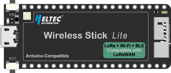
Heltec Wireless Stick Lite (V1 & V3)
|
I originally purchased a couple of Wireless Stick Lite modules as a more economical alternative to the Heltec WiFi LoRa 32 modules I had been using, where I did not need a display. At the time I created the present A4a processor board, I did not realise that the Wireless Stick boards included their own on-board TP4054 battery charging module. It was nonetheless noted that, to use the on-board power management capabilities (all I knew about at the time was the on-board voltage regulator), the board had to be powered through its [JST SH1.25] battery connector. As such, this is the default configuration on the present A4a processor board and requires the battery be directly connected to the Wireless Stick Lite module.
This board includes optional support for:
- [3.3V] power input via Vcc pin (configured via solder jumper)
- EEPROM
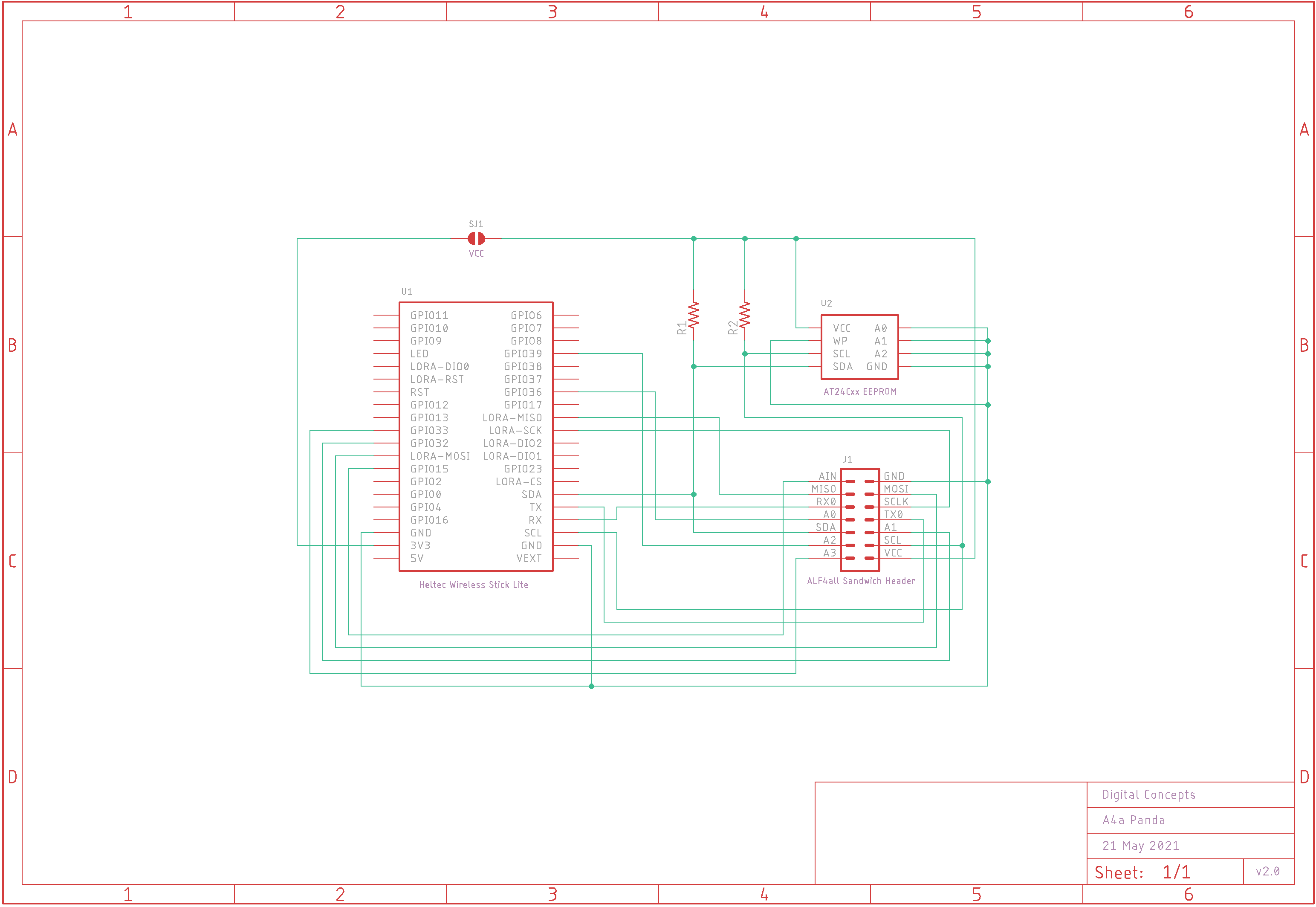
A4a Wireless Stick Lite Schematic
| Top | Bottom |
|---|---|
 |
 |
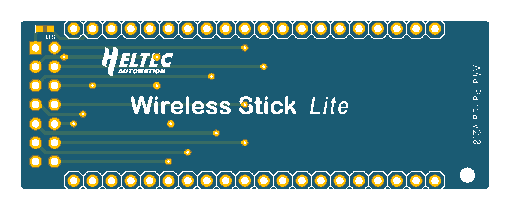
A4a Wireless Stick Lite PCB
Pin Configuration
| Wireless Stick Lite | A4a Sandwich | EEPROM | |
|---|---|---|---|
| Pin | Pin # | Pin | Pin |
| 3V3 (optional) | [1] | VCC | VCC |
| GPIO33 | [2] | A3 | |
| SCL | [3] | SCL | SCL |
| GPIO39 | [4] | A2 | |
| GPIO32 | [5] | A1 | |
| SDA | [6] | SDA | SDA |
| TX | [7] | TxD | |
| GPIO36 | [8] | A0 | |
| LORA-SCK | [9] | SCLK | |
| RX | [10] | RxD | |
| LORA-MOSI | [11] | MOSI | |
| LORA-MISO | [12] | MISO | |
| GND | [13] | GND | GND, A0, A1, A2, WP |
| GPIO15 | [14] | Ain | |
The on-board TP4054 charging circuit, however, obviates the need for the battery management circuitry included on my [BCS-A4a] solar power base boards. On this basis, I may have to rethink my approach to the use of Heltec boards in my current environment. The whole idea of this project was to create a hardware environment where I could swap different processors in and out to see how they compared.
Given the integrated nature of the Heltec boards that I'm working with, I have had to modify my approach to assessing their suitability for individual applications and look at using specific, custom boards for the individual Heltec processor modules. To date, however, I have not created such a board for the Wireless Stick Lite.
While I have generally tended to favour the CubeCell boards in the development of Node (as distinct from Gateway) applications to date, the Heltec WiFi LoRa 32 (V1 & V2) and Wireless Stick [Lite] development boards do, however, retain one particular advantage over the CubeCell boards: they support WiFi and bluetooth communications.
Heltec Wireless Stick Lite V3

|
Like the WiFi LoRa 32 boards, the Wireless Stick Lite V3 Dev-Board is not pin compatible with the earlier V1 Dev-Board (I am not aware of there ever having been a V2 in the Wireless Stick series) but I am in the process of designing a specific 85x58 base board for the V3 Dev-Board, similar to the BHWL3 board, for use with applications that do not require an OLED display. There is currently [Feb 2023] very little guidance on how the newly available pins can be used so, again, the details below are only preliminary—I am yet to test this board or even verify that the new pin connections are valid.

| Top | Bottom |
|---|---|
 |
 |
8558-BHWSL PCB
See here for CAD and CAM files.
Pin Configuration
| Wireless Stick Lite V3 | Solar Panel | EEPROM | I2C |
|---|---|---|---|
| Pin | Pin | Pin | Pin |
| 5V | + | ||
| 3V3/Vext | VCC | VCC | |
| GND | - | GND, A0, A1, A2, WP | GND |
| GPIO20 | SCL | SCL | |
| GPIO19 | SDA | SDA | |
| Wireless Stick Lite V3 | Connector | Note |
|---|---|---|
| Pin | Pin | |
| 3V3 | J1-4/J3-4/J10-1 | |
| 5V | J4[A]-1 | Solar Panel |
| GND | J1-3/J3-3/J4[A]-2/J10-2 | |
| GPIO2 | J11-1 | |
| GPIO4 | J11-2 | |
| GPIO5 | J11-3 | |
| GPIO6 | J11-4 | |
| GPIO7 | J11-5 | |
| GPIO19 | J1-1/J12-1 | SDA |
| GPIO20 | J1-1/J12-2 | SCL |
| GPIO34 | J2-4 | Rain |
| GPIO38 | J8-1 | (Analog) |
| GPIO39 | J8-2 | |
| GPIO40 | J8-3 | |
| GPIO41 | J8-4 | |
| GPIO42 | J8-5 | (Analog) |
| GPIO47 | J2-3 | Wind Direction (Analog) |
| GPIO48 | J2-2 | Wind Speed |
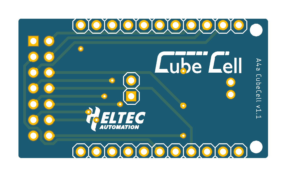
Heltec CubeCell (V1 & V2)

|
The CubeCell includes its own onboard power management circuitry that supports Li-Ion and LiPo battery technology and direct solar panel input—when both are connected directly to the CubeCell module, the solar panel is used to charge the battery. This is the default configuration on the adaptor board below and requires that the CubeCell module be powered via a direct connection from the battery to the CubeCell (JST SH1.25 connector) and that the solar panel, if configured, be connected directly to the CubeCell ALF4all 'Sandwich' processor board (JST PH2.0 connector).
There have been claims that LiFePO4 battery technology is also supported, but these have not been verified—it's not clear how this would be possible, given that the charging regime for LiFePO4 cells differs somewhat from that used for Li-Ion and LiPo cells.
Includes optional support for:
- EEPROM
- Direct power input (configured via solder jumper)
- Solar panel input
| Top | Bottom |
|---|---|
 |
 |
A4a CubeCell PCB
Pin Configuration
| CubeCell | A4a Sandwich | Solar Panel | EEPROM | |
|---|---|---|---|---|
| Pin | Pin # | Pin | Pin | Pin |
| Vin (optional) | [1] | VCC | VCC | |
| GPIO3 | [2] | A3 | ||
| SCL | [3] | SCL | SCL | |
| GPIO2 | [4] | A2 | ||
| GPIO1 | [5] | A1 | ||
| SDA | [6] | SDA | SDA | |
| TX | [7] | TxD | ||
| GPIO0 | [8] | A0 | ||
| SCK | [9] | SCLK | ||
| RX | [10] | RxD | ||
| MOSI | [11] | MOSI | ||
| MISO | [12] | MISO | ||
| GND | [13] | GND | - | GND, A0, A1, A2, WP |
| GPIO5 | [14] | Ain | ||
| VS | + | |||
As I worked through the testing cycle on this board, however, as with the Heltec Wireless Stick, it became apparent that this is not really a very appropriate way to be using the CubeCell, as the module itself includes much of the functionality provided by the [BCS-A4a] solar power base boards. In particular, and quite logically, effective power management through the on-board power management system not only requires direct connection of the battery and solar panel but also the supply of power to any connected sensors.
On this basis, I abandoned further development of this board and have instead designed a base board (initially only for the 85x58 enclosure) specifically for the CubeCell that provides sensor connectivity that is compatible with my current prototyping environment. The current version also includes specific connectors for anemometer and rain gauge sensors.
Includes optional support for:
- Power switch
- Direct power input (configured via solder jumper)
- Solar panel input
- Circuit current monitoring
- 24V Boost converter
- Weather station (anemometer/rain gauge) sensor input
- EEPROM

| Top | Bottom |
|---|---|
 |
 |
8558-BHC PCB
See here for CAD and CAM files.
Pin Configuration
| CubeCell | Solar Panel | EEPROM | I2C |
|---|---|---|---|
| Pin | Pin | Pin | Pin |
| Vext (optional) | VCC | VCC | |
| VS | + | ||
| GND | - | GND, A0, A1, A2, WP | GND |
| TX | |||
| RX | |||
| SCL | SCL | SCL | |
| SDA | SDA | SDA | |
| CubeCell | Sensor |
|---|---|
| Pin | |
| ADC | Wind Direction |
| GPIO0 | Wind Speed |
| GPIO1 | DS18B20 (Temperature) |
| GPIO2 | Sensor Wake |
| GPIO3 | Sensor Interrupt |
| GPIO5 | Rain |
While it uses the ASR6502, rather than ASR6501, processor, the CubeCell Dev-Board V2 is pin compatible with the V1 board and as such is generally interchangeable with the V1 board in the present environment.
Heltec CubeCell Plus

|
The CubeCell Plus board has become the basis for the two specific applications that are currently active. The main feature of interest over the CubCell, which was originally based on the ASR6501 MCU, is that the Plus, which is based on the ASR6502 MCU, includes three ADC channels—this limitation has been alleviated somewhat on the CubeCell V2 Dev-Board, which is now based on the same ASR6502 MCU, although the CubeCell Dev-Board still only provides access to two of the three ADCs. The Plus also includes an inbuilt OLED display, although I hadn't ever anticipated much use for a display on a device that would depend on battery power. Nonetheless, it's simple enough to deactivate the display during 'normal' operations and it has proven useful for 'in field' status checking.
As with the CubeCell, I have developed a board (but in this case, for the 100x68 enclosure) specifically for the CubeCell Plus that provides sensor connectivity that is compatible with my current prototyping environment. Again, as with the CubeCell board, the current version also includes specific connectors for anemometer and rain gauge sensors.
Includes optional support for:
- Power switch
- Direct power input (configured via solder jumper)
- Solar panel input
- Battery voltage/current monitoring
- DS18B20 temperature sensor
- 24V Boost converter
- Weather station (anemometer/rain gauge/I2C/Aux) sensor input
- EEPROM

| Top | Bottom |
|---|---|
 |
 |
10068-BHCP PCB
See here for CAD and CAM files.
Pin Configuration
| CubeCell Plus | Solar Panel | EEPROM | I2C | GPS |
|---|---|---|---|---|
| Pin | Pin | Pin | Pin | Pin |
| Vext (optional) | VCC | VCC | VCC | |
| VS | + | |||
| GND | - | GND, A0, A1, A2, WP | GND | GND |
| UART_TX2 | Rx | |||
| UART_RX2 | Tx | |||
| SCL | SCL | SCL | ||
| SDA | SDA | SDA | ||
| CubeCell Plus | Sensor |
|---|---|
| Pin | |
| ADC1 | Battery (internal) |
| ADC3 | Wind Direction |
| GPIO5 | Sensor Wake |
| GPIO6 | Sensor Interrupt |
| GPIO7 | Rain |
| GPIO8 | Wind Speed |
| GPIO9 | Temperature (DS18B20) |
As with the CubeCell board, this board can be configured with a (100x68) 'weather station' board that provides 'native' (RJ11) connectivity to weather station sensors, with line protection circuitry, as illustrated below.

| Top | Bottom |
|---|---|
 |
 |
10068-WS PCB
With the exception of the NodeMCU and STM32 boards, all of the above described ALF4all processor boards can be accommodated within the 85 x 58 enclosure. The NodeMCU and STM32 processor boards only fit in the larger, 100 x 68 enclosure.
Further Development
As of October 2022, the essential features of all boards have been fully tested. Subsequent development has been largely an exercise in refinement rather than correction of any inherent problems. As I work through the individual boards, I will add the details to the relevant pages under the Assembly menu option at left.
I am also continuing the process of 'refining' the code that's provided under the Software menu option at left. I will continue to 'tidy up' the sketches as I complete the various test cycles and deploy actual applications.