

Boost Converters
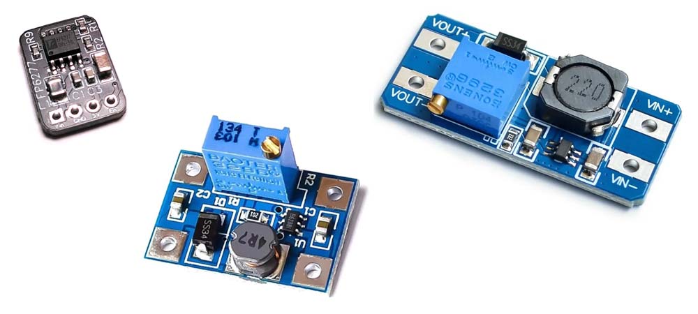
I have used two boost converter ICs in my IoT Nodes. The Aerosemi Technology MT3608 seems to be the most commonly used in boost converter modules available through AliExpress and is capable of providing the 24V output that I needed for one of my sensors. In situations that only require a 5V supply less than 800mA, I have used the Feeling Technology FP6277, for which I found a much tighter packaging option. I have also recently seen the Suosemi SX1308 on AliExpress in a reltively small package that is still claimed to support output voltages up to 28V and 2A, so it might also be worth exploring as a future option.
MT3608
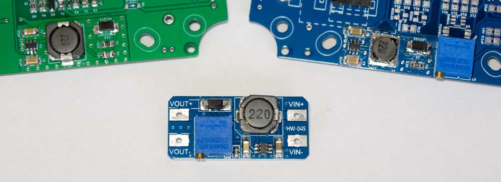
The boost converter configuration included on several base boards described elsewhere on this site (e.g. 10068-BPS, at left in the above photo, and 10068-BCS-A4a, at right) is a direct copy of the circuitry on several commercially available boost converter modules (e.g. that at bottom in the above photo). This configuration can boost the voltage supplied by a [3.7V] Li-Ion battery up to ~28V, depending on the relevant resistor configuration. The commercial modules, and my general configuration, e.g. that used on the 10068-BCS-A4a board, include a trim pot to allow the output voltage to be tuned within this range to that required by any given application.
I have subsequently modified the circuit slightly by adding an extra resistor to the output circuit to provide more sensitivity in setting voltage levels. The original configuration, as per the commercially available module, used a 100kΩ trimpot, but only about 20% of its range was useful. By inserting the additional resistor and using a 10kΩ trimpot, most of the range of the trimpot can be used, allowing the output voltage to be set more precisely.
Circuit Layout
The specific components used, and their layout, in a boost converter circuit can be a little fussy. Apart from the need to observe the guidelines provided in the relevant datasheet, in my applications care needed to be taken in choosing the physical size of some components. It may have been immediately obvious to someone with more experience in such matters, but I ultimately discovered that the physical size, not just the rating, of the inductor and output capacitor had an impact on the maximum current that could be delivered through the boost converter circuit.
In my initial attempts to keep the layout as compact as possible, I just arranged what I thought were appropriately rated components neatly on the relevant PCB. Unfortunately, these early configurations were quite unstable and never delivered the expected 24V output. When I paid more attention to the layout guidance provided in the MT3608 datasheet the results were more positive.
I encountered another problem when developing the 10068-BPS battery board to support a Raspberry Pi Zero. Once again to save space, I had used a smaller [CDRH6D28] inductor and [0805] output circuit capacitor only to discover that, while the voltage level was fine, this configuration could not deliver the required current. Using the same sized [CDRH104R] inductor and [1206] capacitor as the commercially available module, which I had successfully used to test the capability before designing my own PCB, solved this problem.
I also fried a Raspberry Pi Zero early on with an incorrectly set trim pot so, for that particular application, the green board at left in the photo above, I dispensed with the trim pot and just used a fixed resistor configuration to deliver the required 5V.
Output Voltage
From the MT3608 datasheet, the output voltage is determined by the values of the resistors in the output side of the boost converter circuit, according to the following equation:
`V_(out) = V_(ref)\times (1 + (R1)/(R2))`
where the internal reference voltage Vref is typically 0.6V and the values of R1 and R2 are determined, in our case, by the values of resistors R1 and R2 and the setting of the trimpot R1/2.
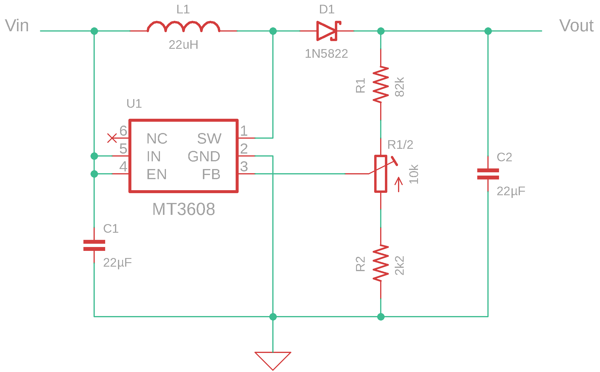
Boost Converter Circuit
The MT3608 IC operates on an input voltage in the range 2~24V and generates an output voltage up to 28V. The following table lists the theoretical output voltage across the range of the 10kΩ trimpot.
Theoretical Vout Values
| R1 | R2 | Vout (V) | ||
|---|---|---|---|---|
| R1 (kΩ) | Trimpot (kΩ) | R2 (kΩ) | ||
| 82 | 10 | 0 | 2.2 | 28.4 |
| 9 | 1 | 19.5 | ||
| 8 | 2 | 14.9 | ||
| 7 | 3 | 12.0 | ||
| 6 | 4 | 10.1 | ||
| 5 | 5 | 8.7 | ||
| 4 | 6 | 7.6 | ||
| 3 | 7 | 6.8 | ||
| 2 | 8 | 6.1 | ||
| 1 | 9 | 5.6 | ||
| 0 | 10 | 5.1 | ||
Details relating to individual circuit components are provided under the PCB Assembly pages elsewhere on this site.
MT3608 Daughter Board
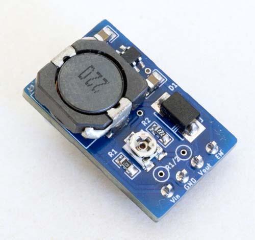
This is actually the last of the three boost converter daughter boards discussed here that I created. I did this primarily to have an option with a configurable output voltage. Even though the MT3608 and SX1308 are essentially identical, this was also, in part, an exercise in moving the boost converter circuit that I had configured on some base boards (e.g. on the 10068-BCS-A4a) onto a daughter board, so I used essentially the same components that had been used there (see here for PCB CAD and CAM files).
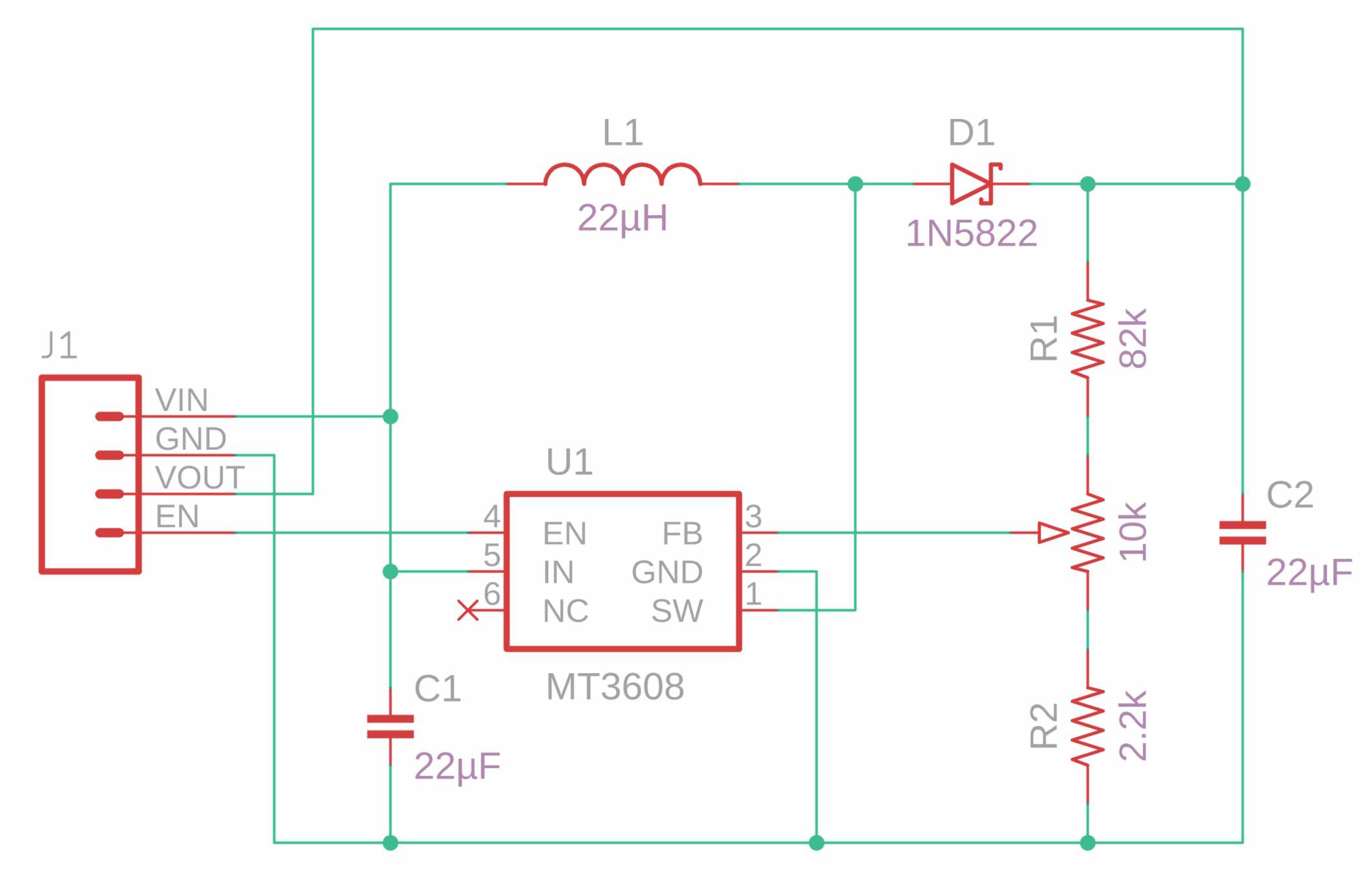
MT3608 Boost Converter Module Circuit
While this module uses the same header configuration as the other two, it has a slightly larger form factor, as a result of the inclusion of the trimpot and use of a physically larger inductor. While the trimpot is not as finely adjustable as the larger, Bourns (or similar) trimpot used on the base board configurations and commercially available modules, the function of this module is identical to those MT3608 configurations.
Assembly
There are no particular issues of note in assembling this module except, perhaps given the compact form factor used, the order in which the components are assembled. I have found the following sequence provides good access to individual components if they are being hand soldered:
- MT3608
- R1 & R2
- Trimpot
- 1N522
- C1 & C2
- Inductor
- Header
FP6277 Daughter Board
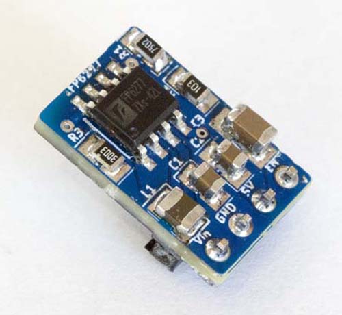
My initial boost converter daughter board was a version of the compact module designed by Gerrit Niezen as a solution that could simply be plugged into a Node if and when required (see here for PCB CAD and CAM files). In particular, the Niezen design uses a chip inductor that is much smaller than than the more common and larger wire wound items.
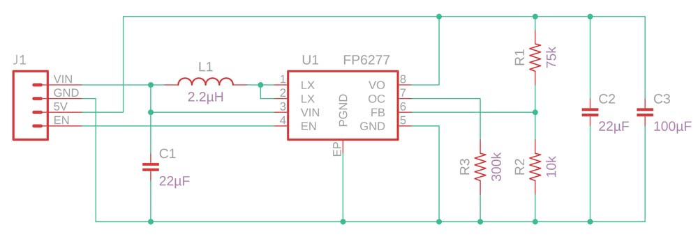
FP6277 Boost Converter Module Circuit
The FP6277 IC operatres on an input voltage in the range 2.4~4.5V and generates an output voltage up to 5.3V with a current limit of 800mA in the present configuration. The current limit for the FP6277 is set via the resistance configured on the OC pin and, once again, the output voltage is set according to the values of the resistive voltage divider connected to the FB pin of the IC:
`V_(out) = V_(ref)\times (1 + (R1)/(R2))`
The enable pin [on the FP6277] is pulled HIGH to switch the IC ON, LOW to switch it OFF.
Assembly
One critical requirement that I encountered with the FP6277 was that the ground pad on the bottom of the IC must be soldered to the ground plane of the PCB—it's not enough for it to just be in contact with the pad on the PCB.
Given the small size of the PCB and component involved, this turned out to be relatively straightforward process using solder paste and the heat gun on a small rework station to apply the necessary heat from the bottom of the PCB. It's also best to do this first, to avoid having other components move around when the board is heated.
This complication, of course, does not exist with either the MT3608 or SX1308 ICs because their packaging does not include such a pad.
SX1308 Daughter Board
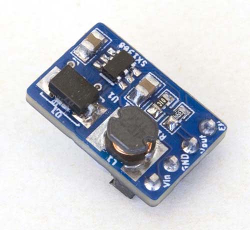
The SX1308 offers an alternative to the MT3608 for voltages up to 28V. The present module (see here for PCB CAD and CAM files) is an implementation of the basic application circuit presented in the SX1308 datasheet. The module is built on the same form factor as the FP6277 module above, with the idea that host board could use either, depending on the needs of configured peripherals.
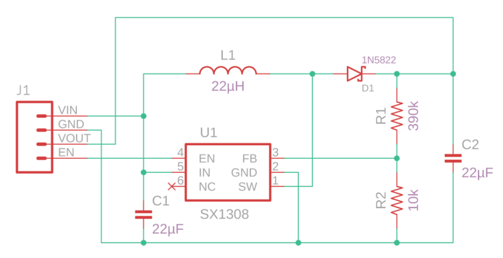
SX1308 Boost Converter Module Circuit
The SX1308 IC operatres on an input voltage in the range 2~24V and generates an output voltage up to 28V with a current limit of 4A. The output voltage is once again set according to the values of the resistive voltage divider connected to the FB pin of the IC:
`V_(out) = V_(ref)\times (1 + (R1)/(R2))`
As for the FP6277, the enable pin [on the SX1308] is pulled HIGH to switch the IC ON, LOW to switch it OFF.
While I have only built a 24V version to date, the SX1308 could also be configured to deliver any voltage in the 5~28V range by simply using an appropriate resistor combination. As such, it may be that this is the only module we need, albeit with several different resistor configurations, for applications that require a supply voltage greater than that delivered by the battery.
The SX1308 initially looked like a more attractive option because the module in the photo at the top of this page presented a smaller package than the MT3608 module. The SX1308 and MT3608 ICs are, however, interchangeable—their respective datasheets are word for word and illustration for illustration identical.
Assembly
There are no particular issues of note in assembling this module. I originally created the FP6277 module described above because I thought it would be easier to hand solder 0805 SMD components than the smaller 0603 ones used in the original Neizen design. In the event, while the 0805 components are bigger and easier to work with, soldering 0603 components like the resistors on the present module did not turn out to be as difficult as I imagined it might be.