100 × 68 Boards
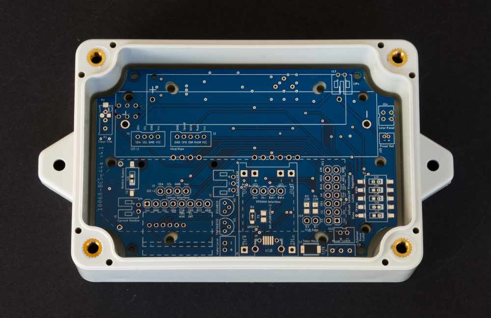
The following is a selection of the 100 × 68 enclosure boards that I currently use, or have used, in various applications.
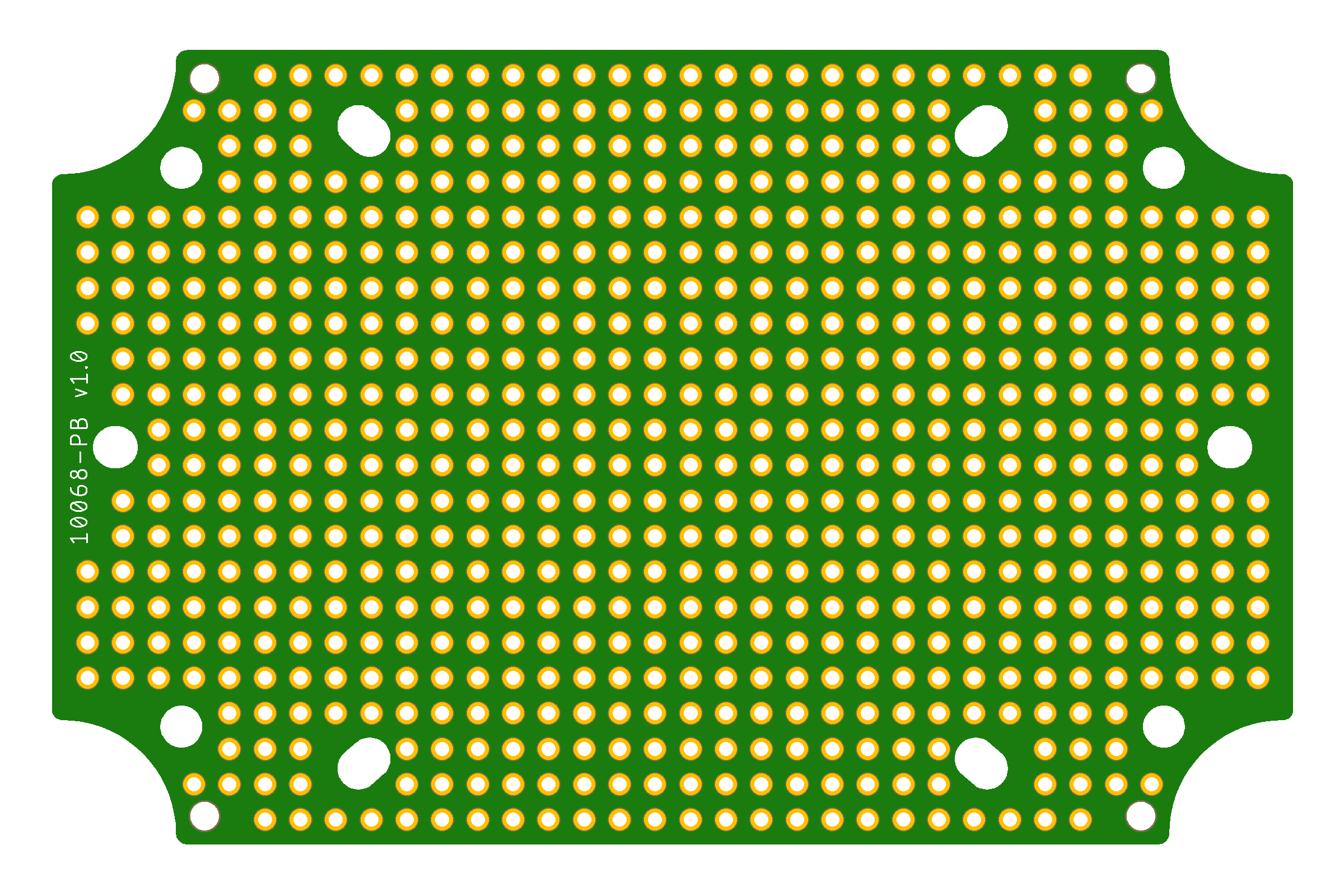
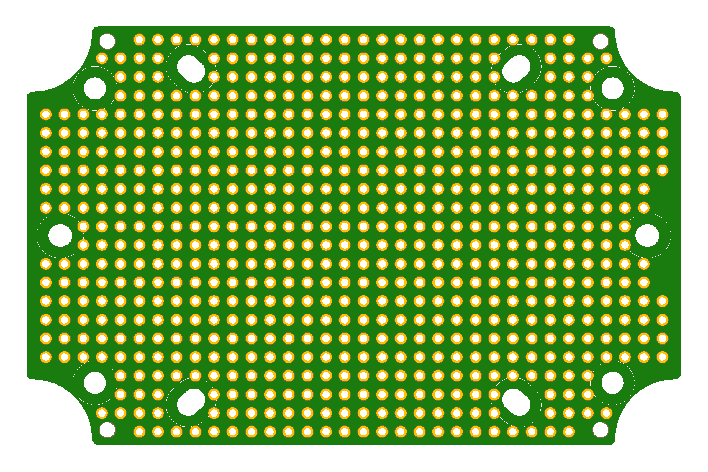
[10068-PB] Simple Prototyping Pad Matrix
| Top | Bottom |
 |
 |
10068-PB PCB
[10068-PBC] Prototyping Base with edge Cut-outs
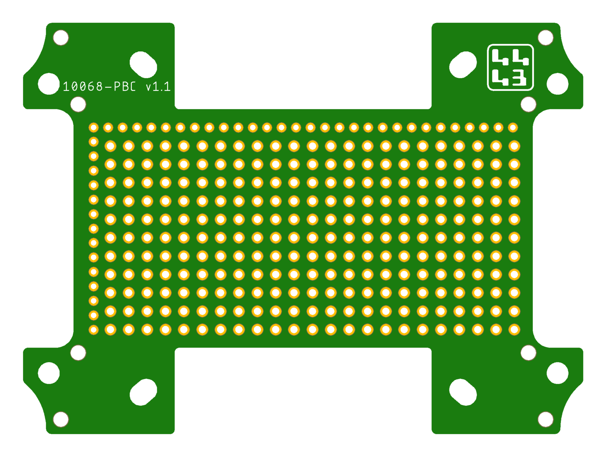
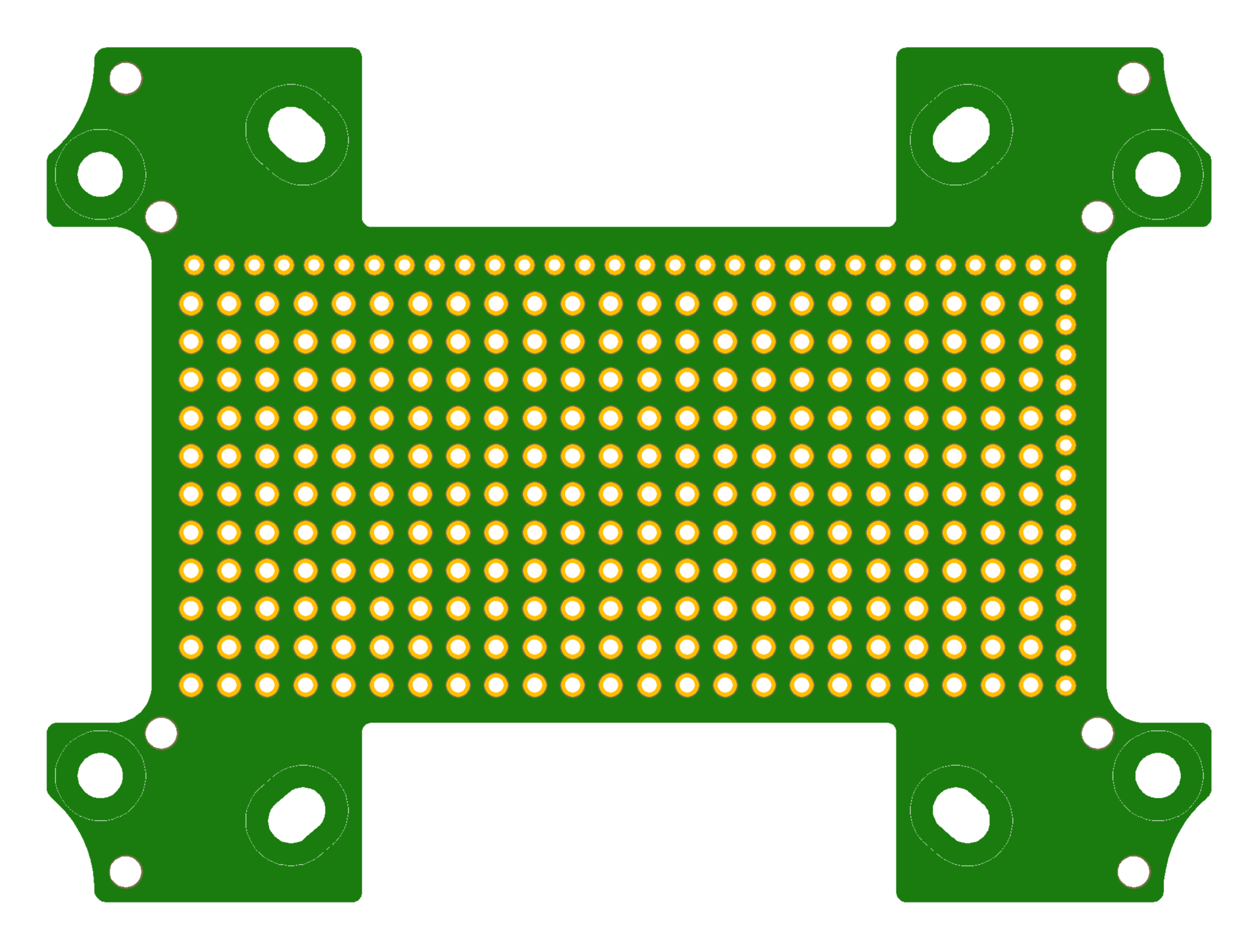
In assembling various node configurations, I often needed to include external connectors. This was not generally a problem with the larger enclosures as there was plenty of room in the 40/50 mm enclosure wall. But with some of the the more complex, stacked configurations the external connectors, which often protruded into the enclosure further than the edge of the standard shaped PCB, came into conflict with the enclosure contents.
To handle such situations, I created a board with cut-outs along the edges. I tend to use this board as the bottom board in a stack, providing the necessary room for external connectors that could be located low down in the wall of the enclosure so as not to interfere with any of the higher, generally component-bearing boards in the stack.
While the board is designed for a 100 × 68 enclosure, it includes 'stack mounting holes' for both 85 × 58 and 100 × 68 stacking boards described on this site.
I also included a 100 mil pad matrix in the 'middle' of the board, and then a column and row of 2 mm spaced pads to support PH 2.0 connectors, just because I could.
| Top | Bottom |
 |
 |
10068-PBC PCB
[10068-PBLPI] Battery Mounts, Power 'Rails' and Edge Links
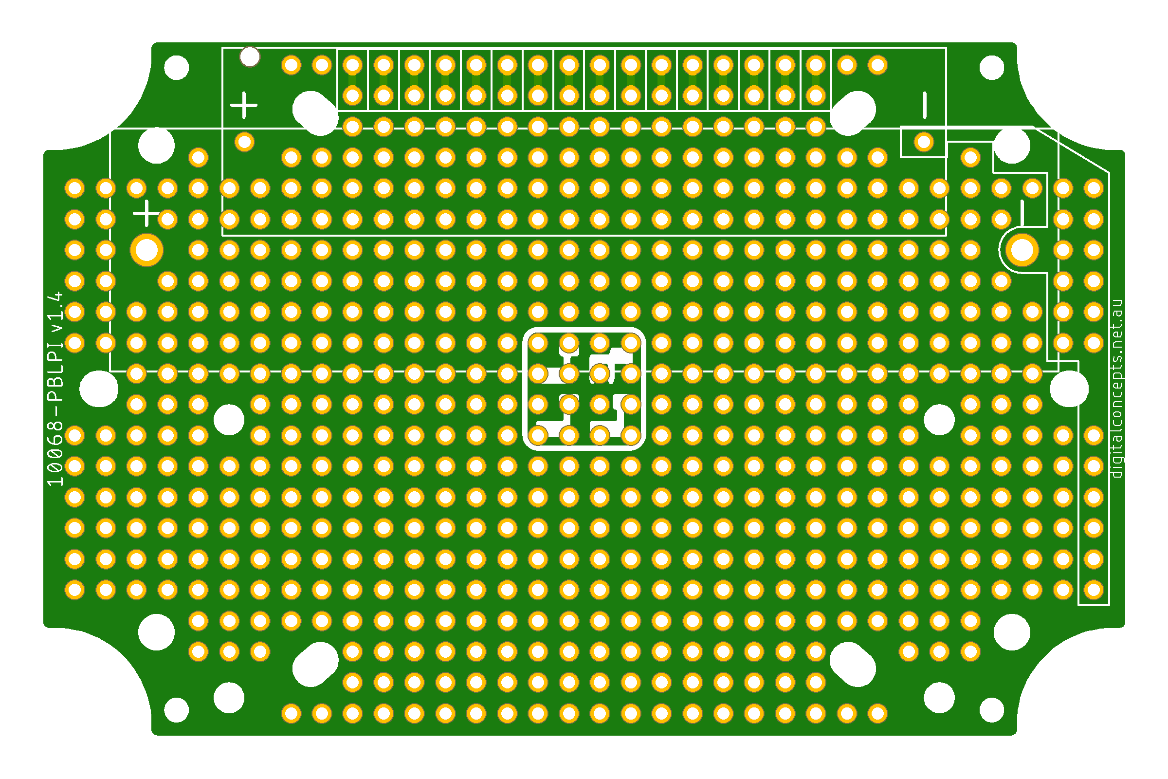
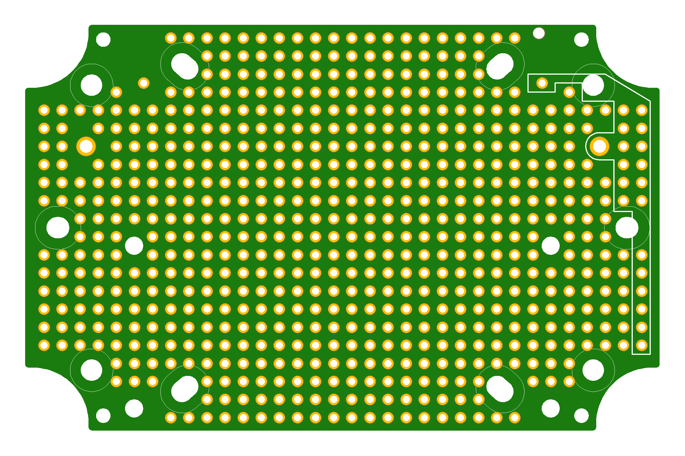
This is the current version of my first prototyping board. In addition to a standard 100 mil pad array, this board includes mount points for 14500 (AA) and 18650 battery holders, connected to Vcc/GND power 'rails'. It also includes a series of connected pad pairs along one edge and mounting holes for a Raspberry Pi Zero.
Board schematic
| Top | Bottom |
 |
 |
10068-PBLPI PCB
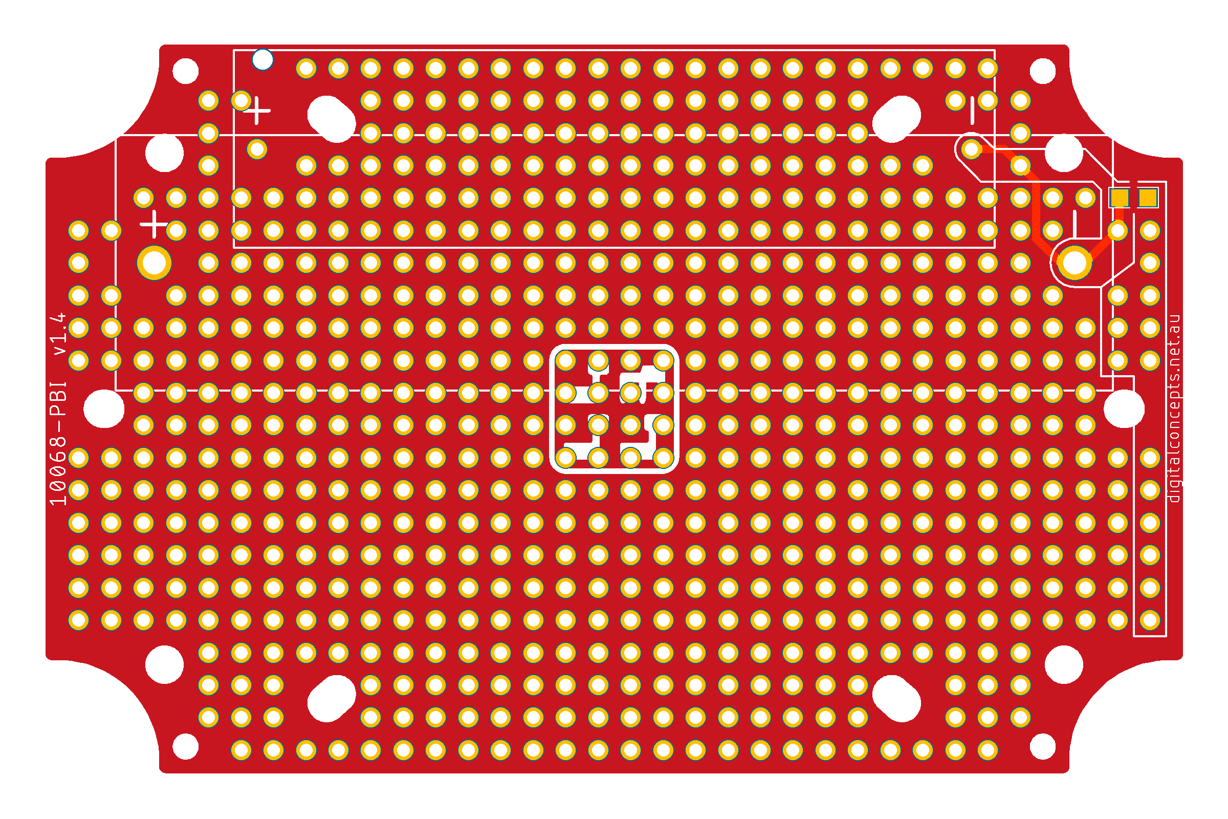
[10068-PBI] Battery Mounts and Jumpered Power 'Rails'
In addition to a standard 100 mil pad array, this board includes mount points for 14500 (AA) and 18650 battery holders, with jumper-configured power 'rails' (Vcc/GND).
Board schematic
| Top | Bottom |
 |
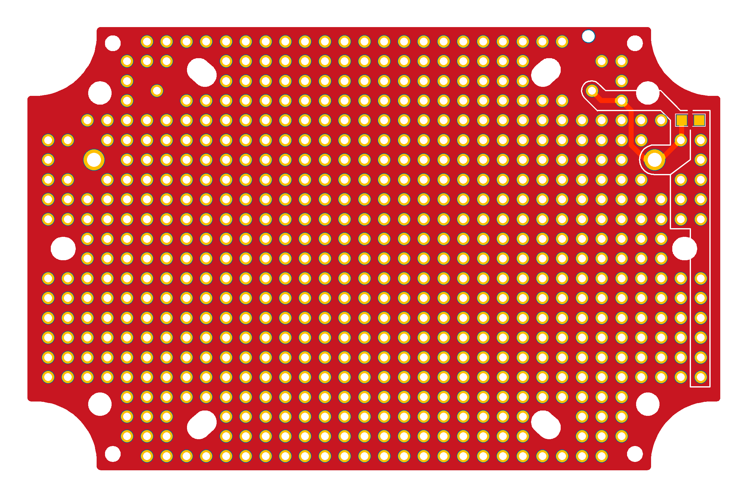 |
10068-PBI PCB
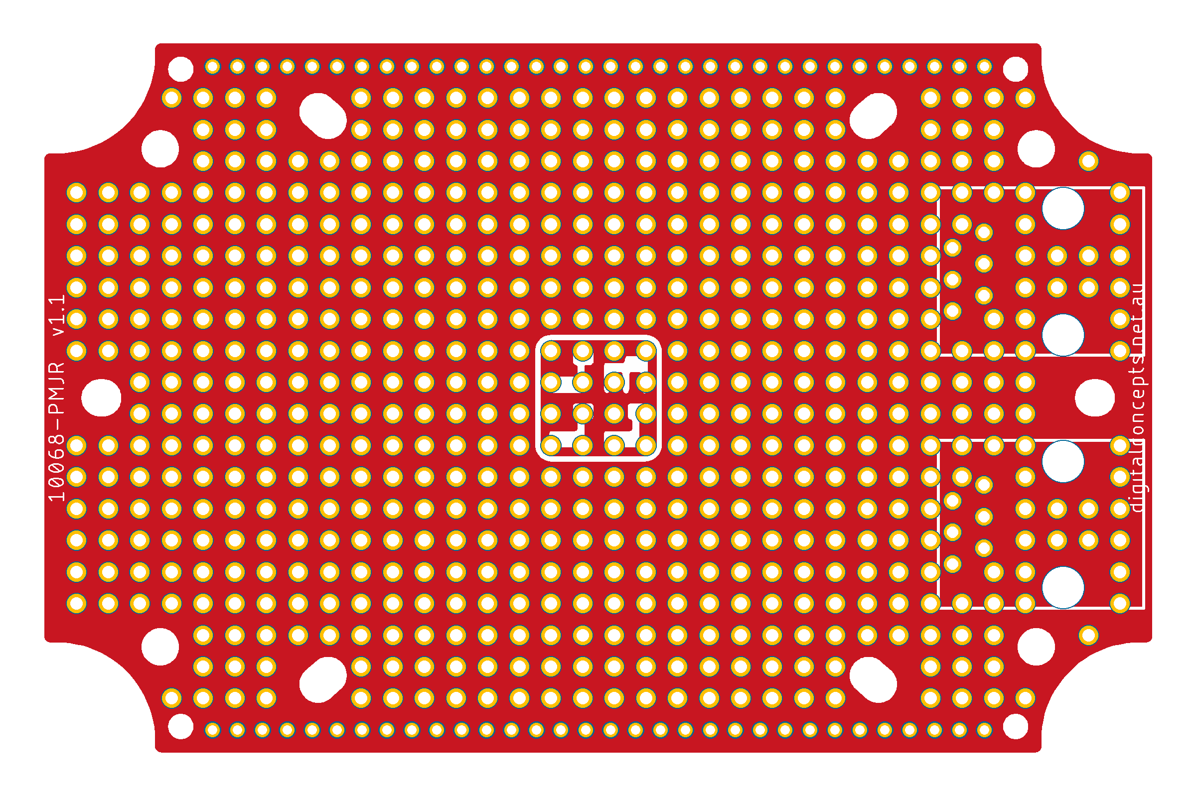
[10068-PMJR] PH2.0 (JST) and RJ11 (vertical) Mounts
In addition to a standard 100 mil pad array, this board includes pads at 2 mm spacing, suitable for JST PH2.0 connectors, along the long edges and mount points for two vertical RJ11 (6P6C) connectors.
Board schematic
| Top | Bottom |
 |
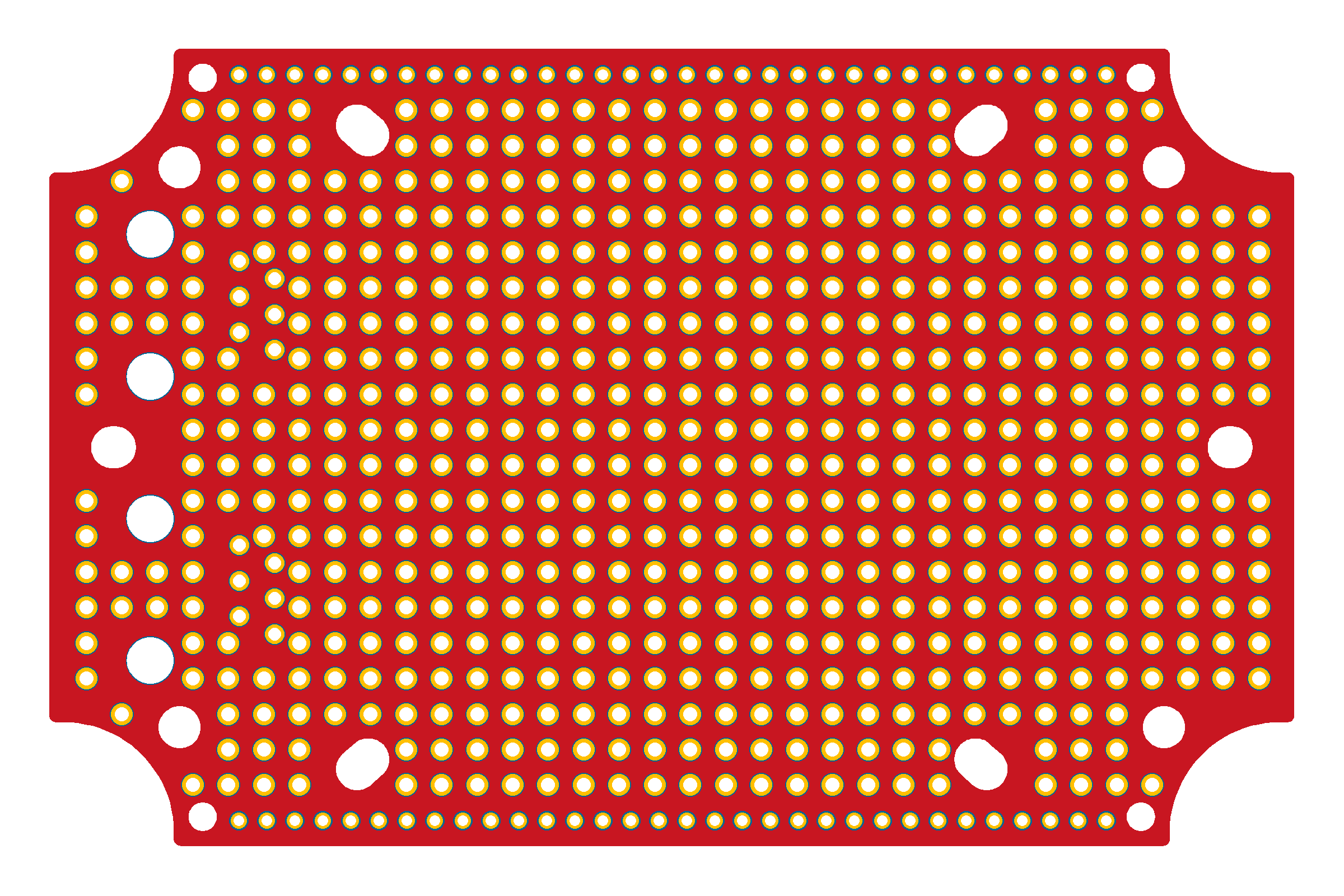 |
10068-PMJR PCB
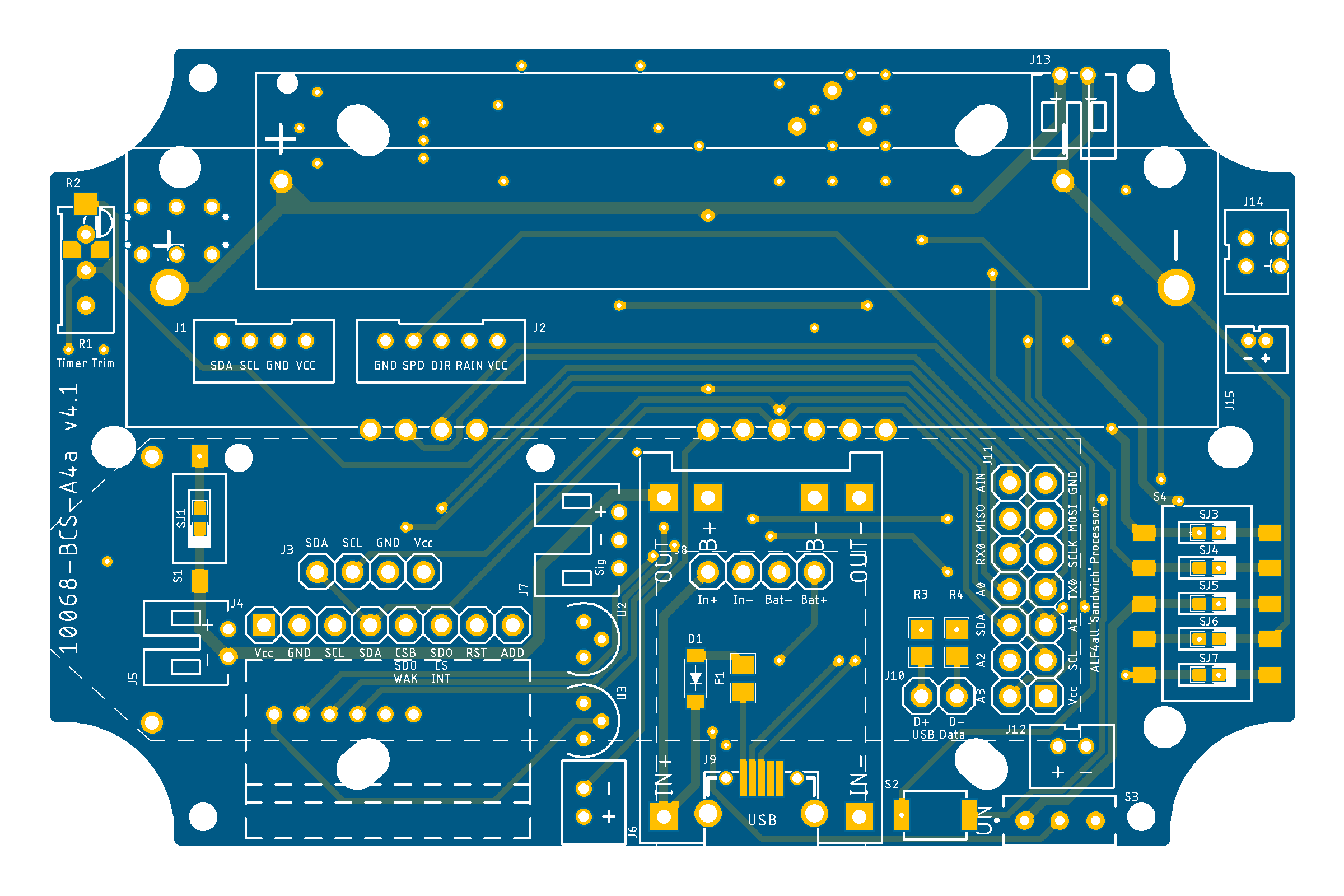
[10068-BCS-A4a] IoT Node Power/Sensor Prototyping Board
This is my current IoT node prototyping board. Most of the features on the board are optional—they can actually be configured, but switched in/out via DIP switches, allowing for the testing of different board configurations for different applications. A detailed discussion of all of the board features is provided elsewhere on this website (under the section dedicated to IoT node development).
Board schematic
| Top | Bottom |
 |
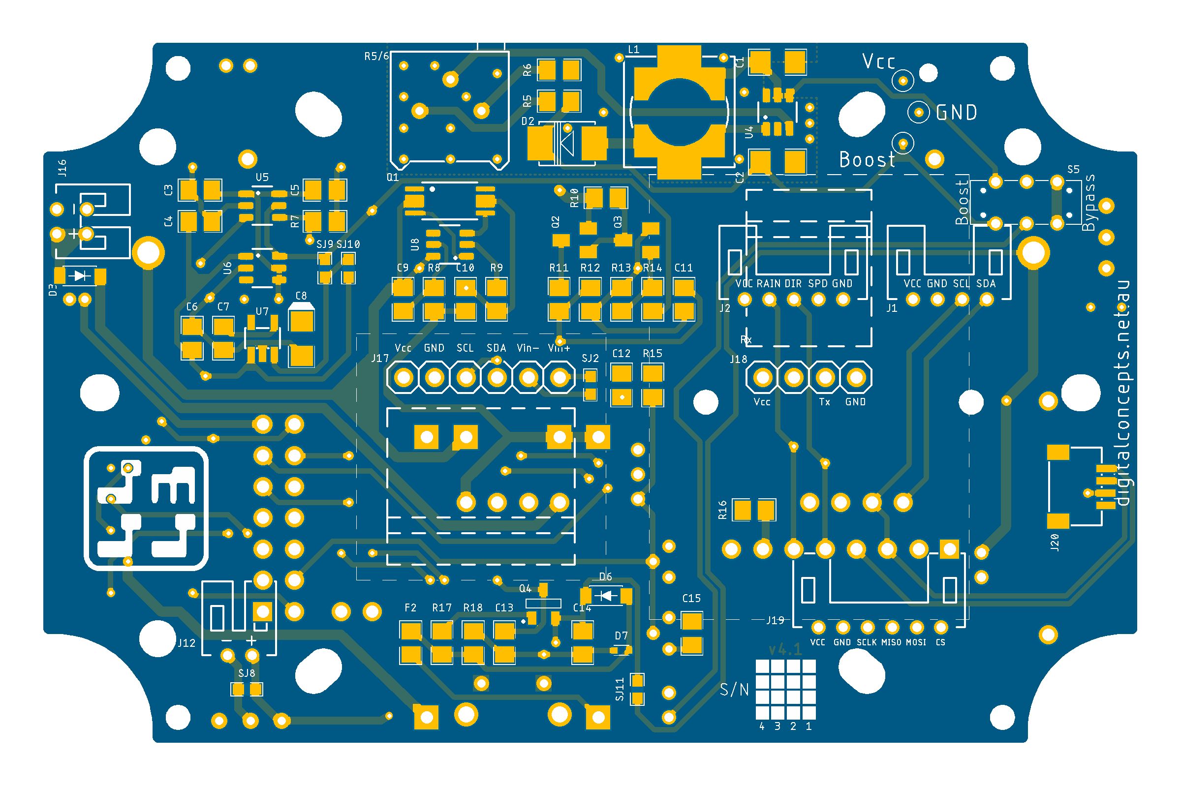 |
10068-BCS-A4a PCB
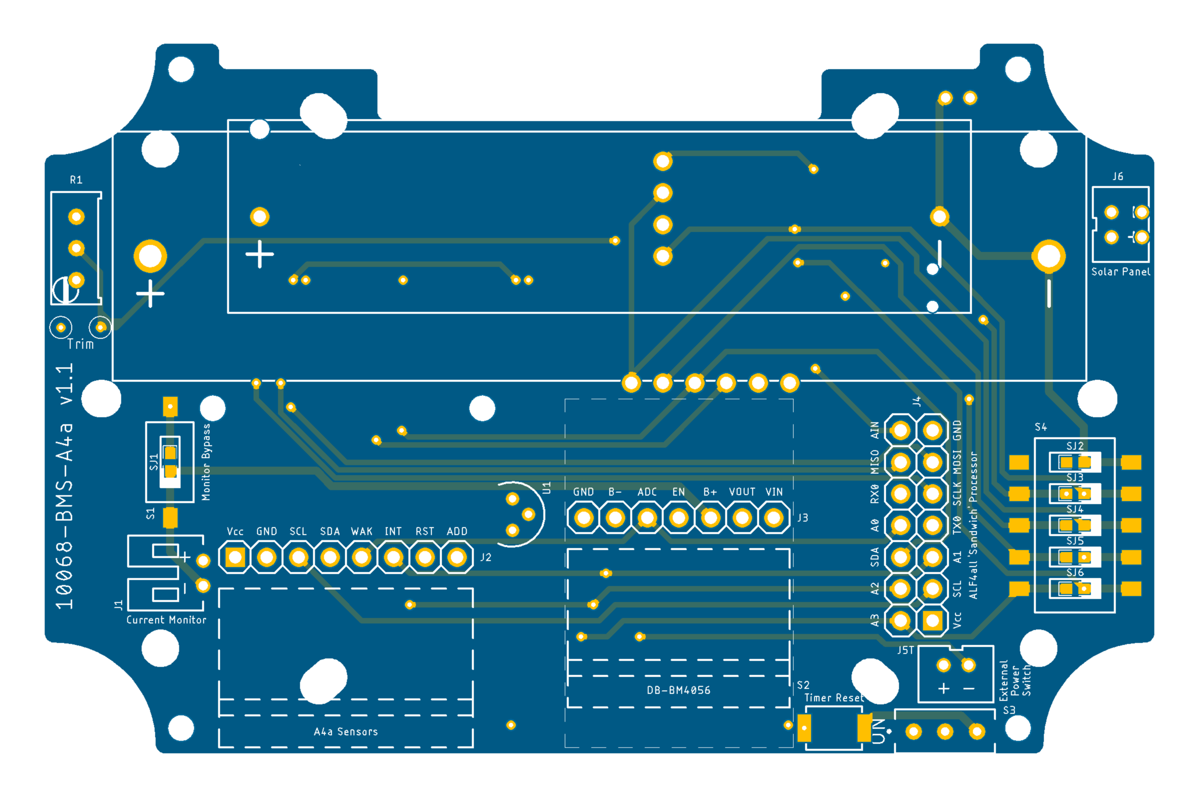
[10068-BMS-A4a] IoT Node Power/Modular Sensor Board
The BMS board is a development of the original BCS board that more directly supports the modular nature of the Node hardware configurations described on this site.
In addition to moving the battery management and boost converter functions to [reusable—a practical consideration when prototyping] daughter boards, this board includes a cut-out along one side to better accommodate external connectors in an enclosure. With most of my Nodes now built on a 'board stack', with sensor interfaces often on a separate board, JST connectors are included to provide generic off-board connectivity to the available processor pins.
Board schematic
| Top | Bottom |
 |
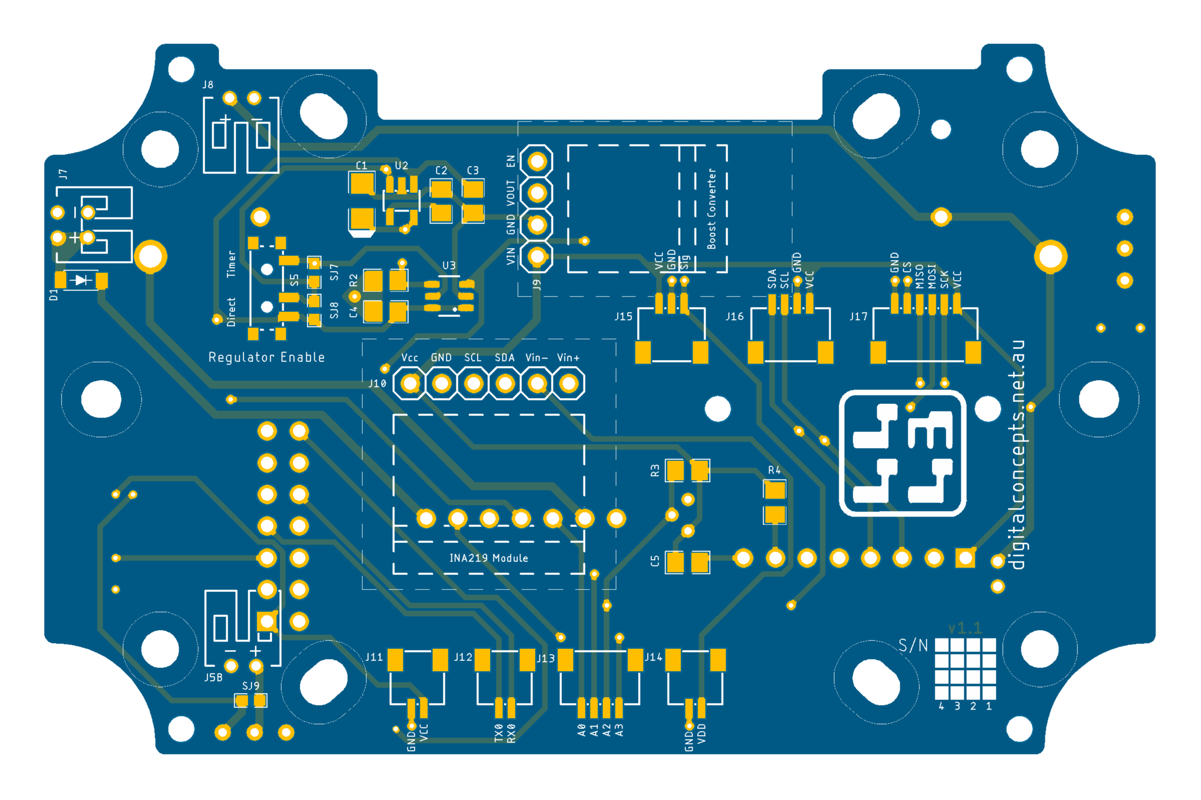 |
10068-BMS-A4a PCB
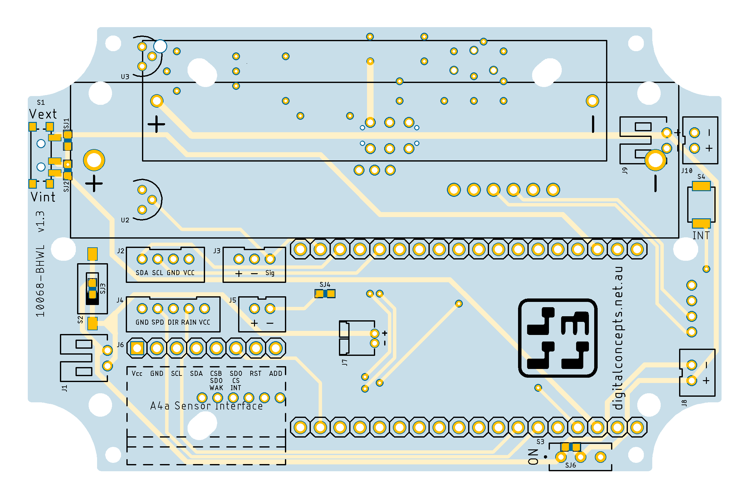
[10068-BHWL] WiFi LoRa 32 Sensor Board
This is a power/sensor board specifically designed for the Heltec WiFi LoRa 32 development board, given that the Heltec boards include their own on-board power management circuitry. A detailed discussion of all of the board features is provided elsewhere on this website (under the section dedicated to IoT node development).
Board schematic
| Top | Bottom |
 |
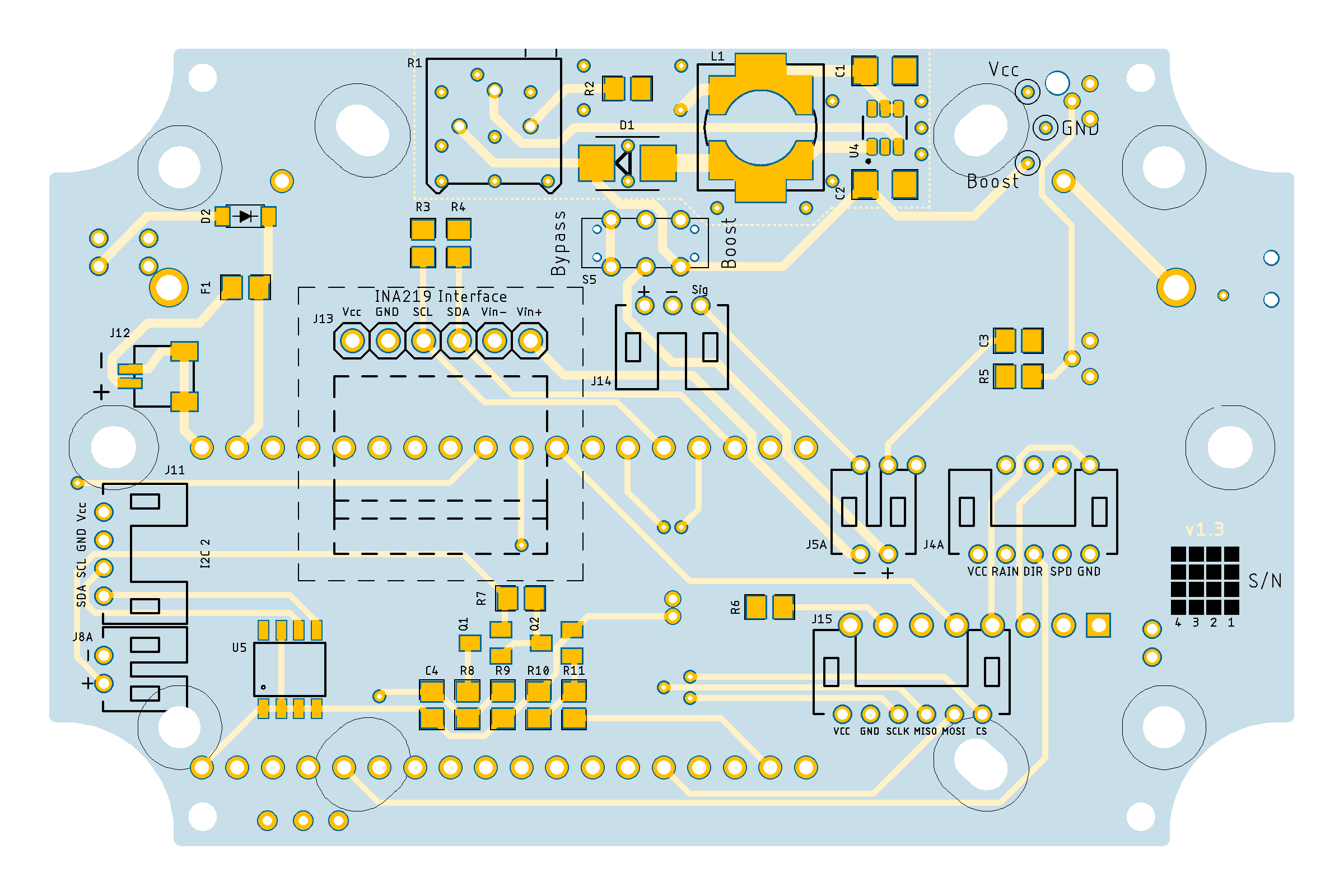 |
10068-BHWL PCB
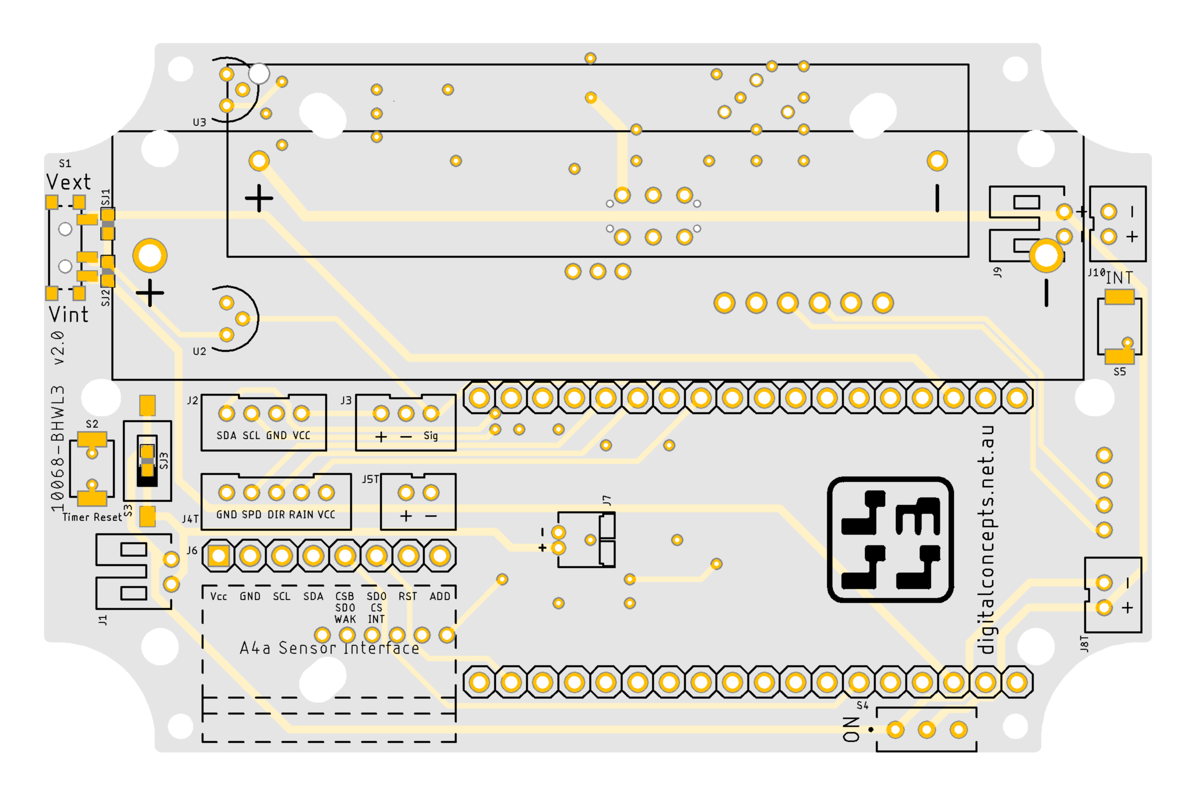
[10068-BHWL3] WiFi LoRa 32 V3 Sensor Board
The Heltec WiFi LoRa 32 V3 development board has much the same physical appearance as the V1 and V2 boards but is based on more recent ESP32-S3 MCU and SX1262 LoRa Node chip and has a completely different pin configuration. The 10068-BHWL3 1.0 board provides the same features as the 10068-BHWL v1.3 board (refer to the section dedicated to IoT node development). Any subsequent updates, given that the V1 & V2 boards have been discontinued, will only be applied to the BHWL3 board.
This board is yet to be fully tested, although individual circuit subsections have been transferred directly from earlier, fully tested versions of the BHWL board.
Board schematic
| Top | Bottom |
 |
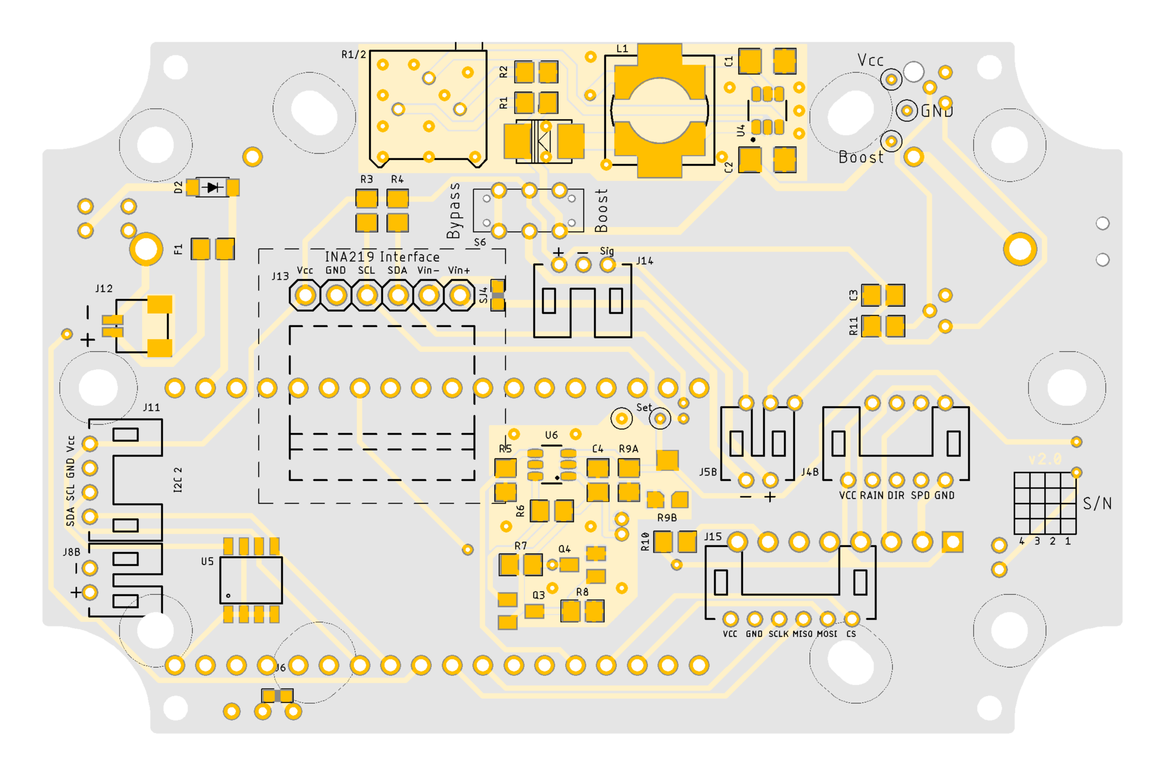 |
10068-BHWL3 PCB
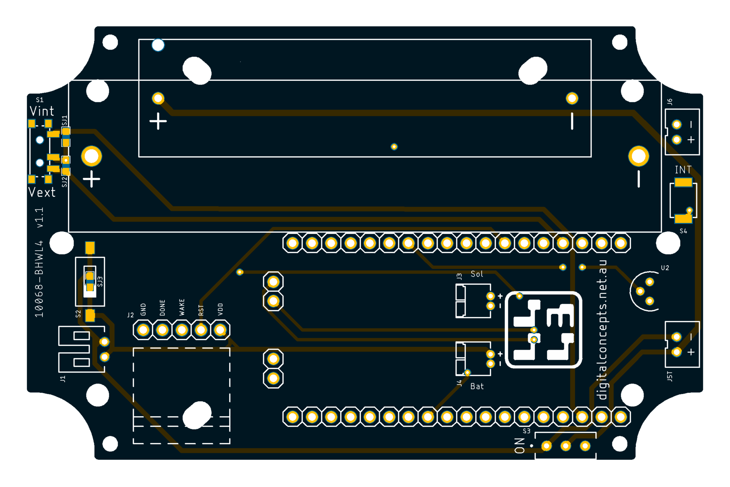
[10068-BHWL4] WiFi LoRa 32 V4 Base Board
The Heltec WiFi LoRa 32 V4 development board is essentially a complete redesign of the WiFi LoRa 32 board, the features of which are discussed on the Platforms page elsewhere on this site. As a consequence, the configuration of the BHWL4 board is a departure from and a complete redesign of previous BHWL boards.
In its most basic configuration, in addition the battery, solar and external power sources, it includes a header for the watchdog timer daughter board. The board no longer includes a boost converter as this is now more often configured on an auxiliary sensor support board. The BHWL4 board then provides off-board connectivity to available processor pins through a series of JST connectors.
Board schematic
| Top | Bottom |
 |
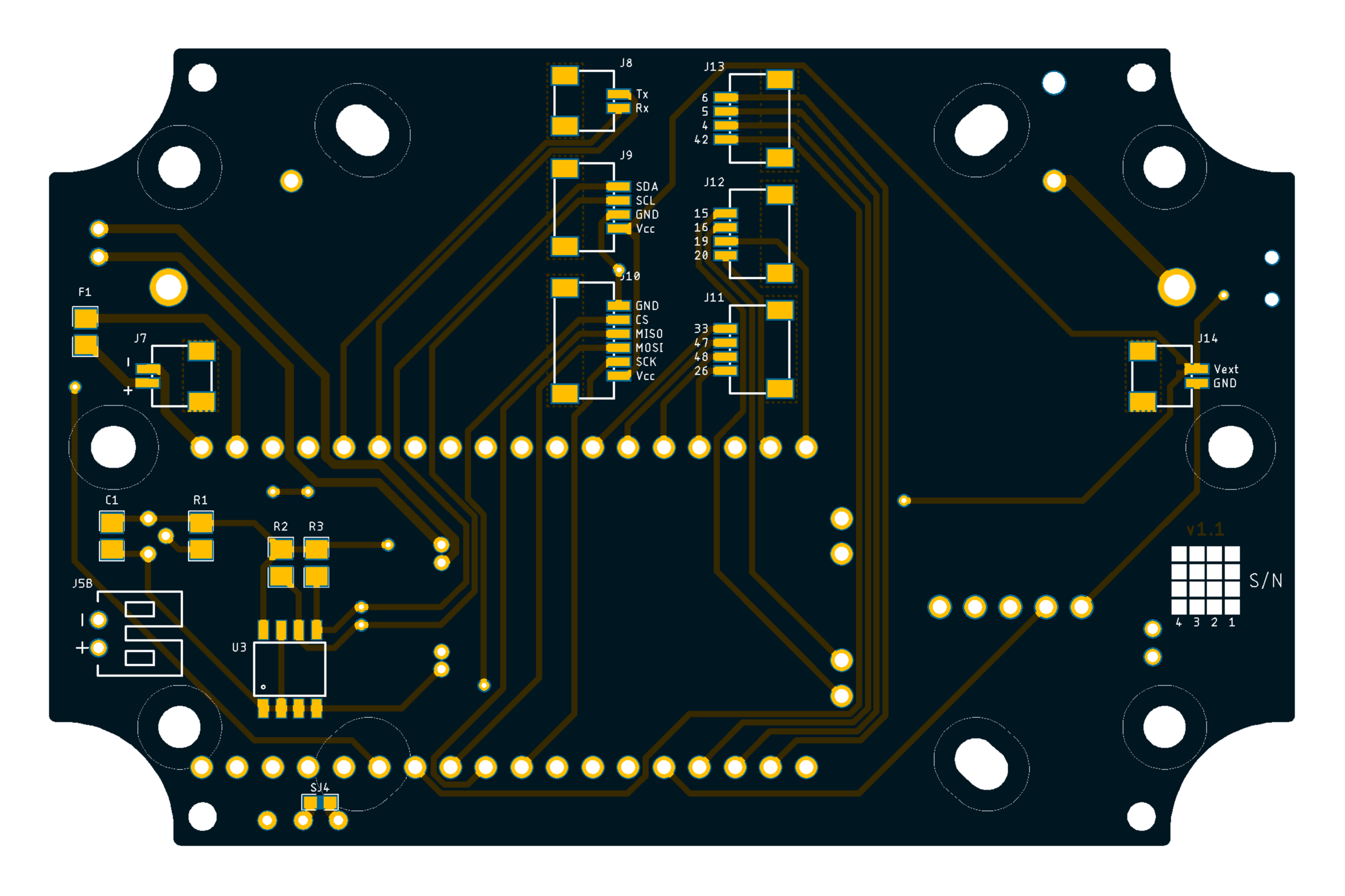 |
10068-BHWL4 PCB
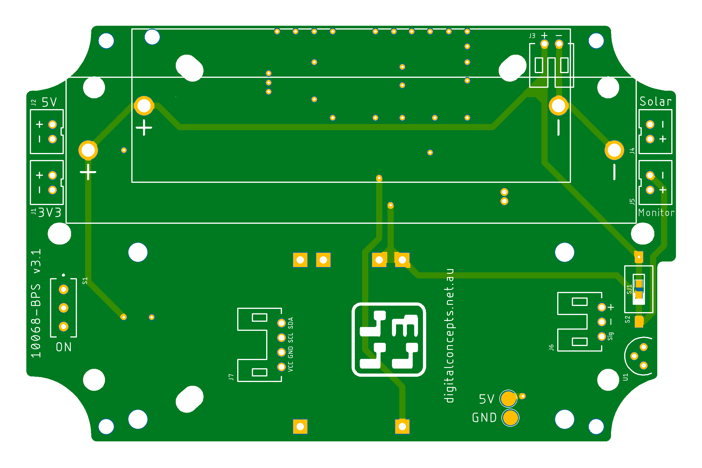
[10068-BPS] Battery Power Supply Board
This is a power supply board primarily designed to provide [backup] battery power for a Raspberry Pi Zero [W] processor. A detailed discussion of the board features is provided elsewhere on this website (under the section dedicated to IoT node development).
This is a new board and is yet to be fully tested.
Board schematic
| Top | Bottom |
 |
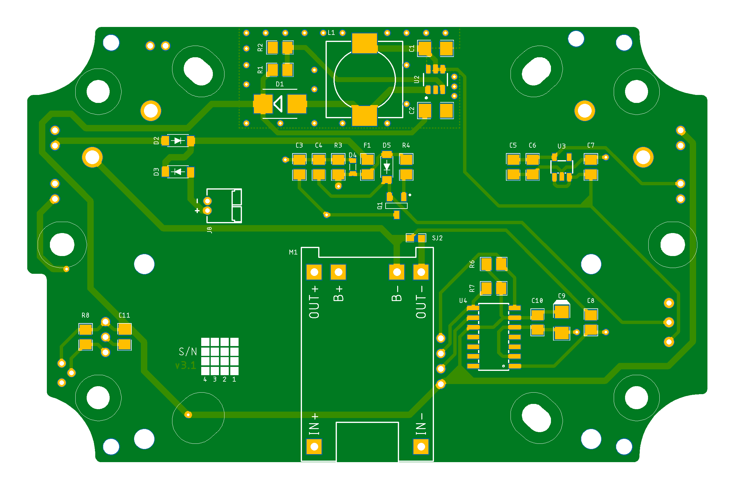 |
10068-BHCP PCB
[10068-BHCP] CubeCell Plus Sensor Board
This is a power/sensor board specifically designed for the Heltec CubeCell Plus development board, given that it includes its own on-board power management circuitry. A detailed discussion of all of the board features is provided elsewhere on this website (under the section dedicated to IoT node development).
Board schematic
| Top | Bottom |
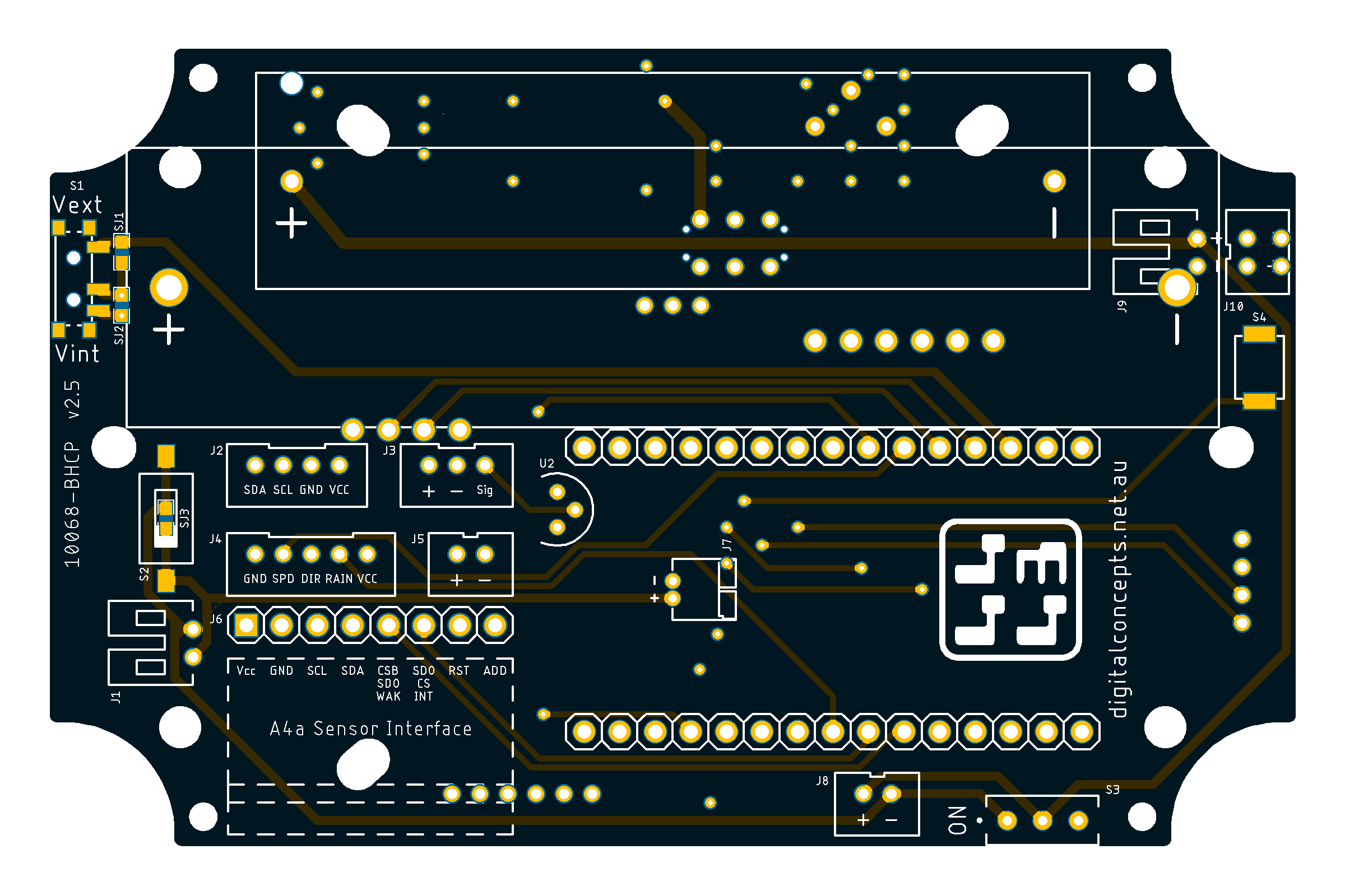 |
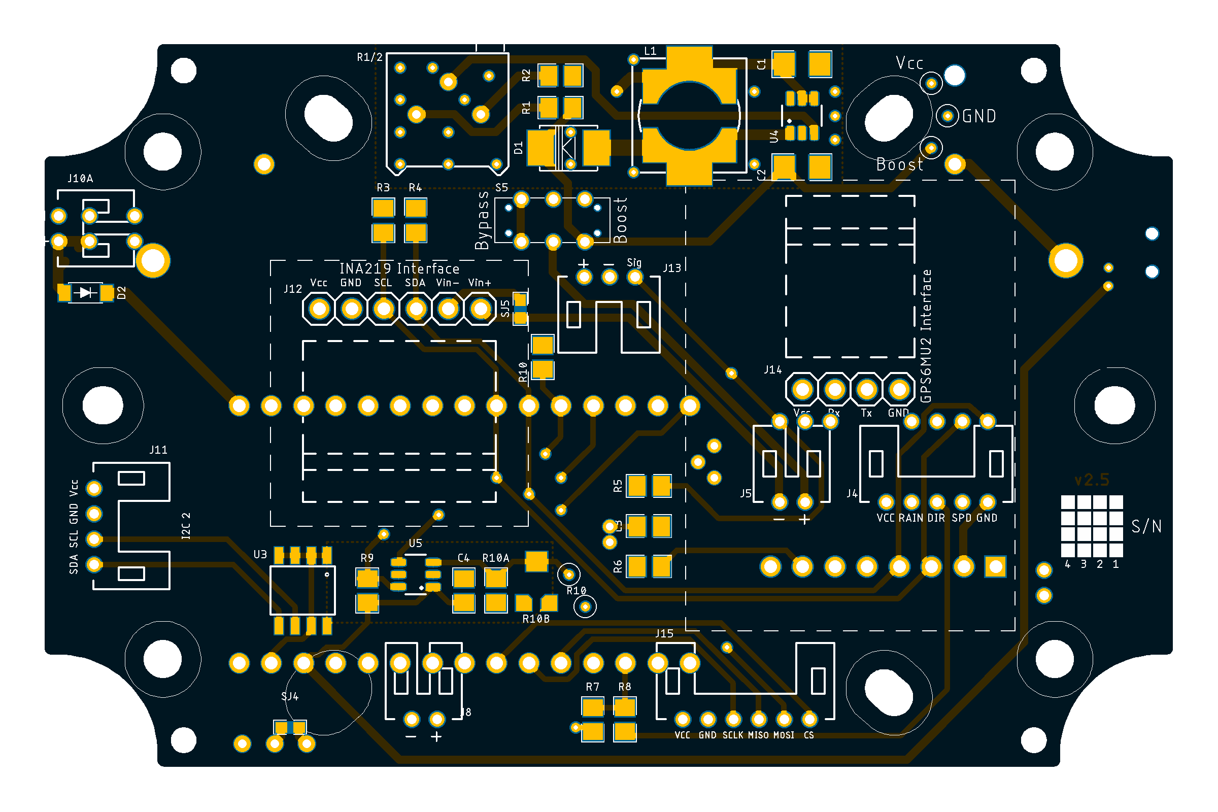 |
10068-BHCP PCB
[10068-GPSJ] GPS Antenna Mount
This board was specifically designed to provide a mounting point for the NEO-6/7/8M GPS module antenna. The rest of the board incorporates a 100 mil pad array and mount points for two JST PH2.0 connectors (suitable for an I2C interface or the like) for additional prototyping work.
Board schematic
| Top | Bottom |
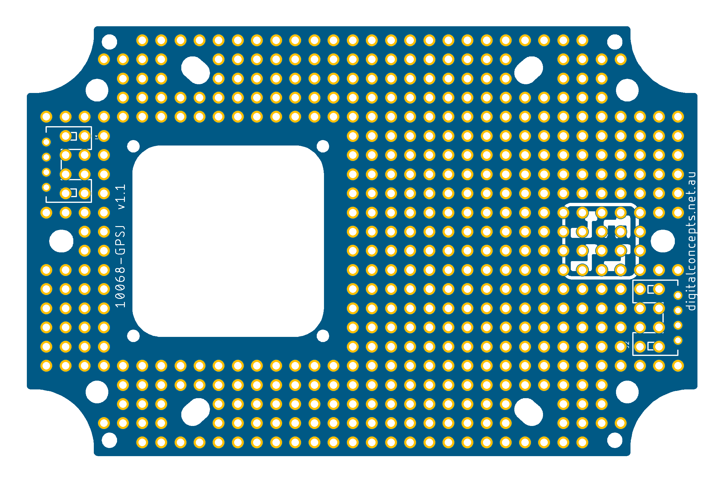 |
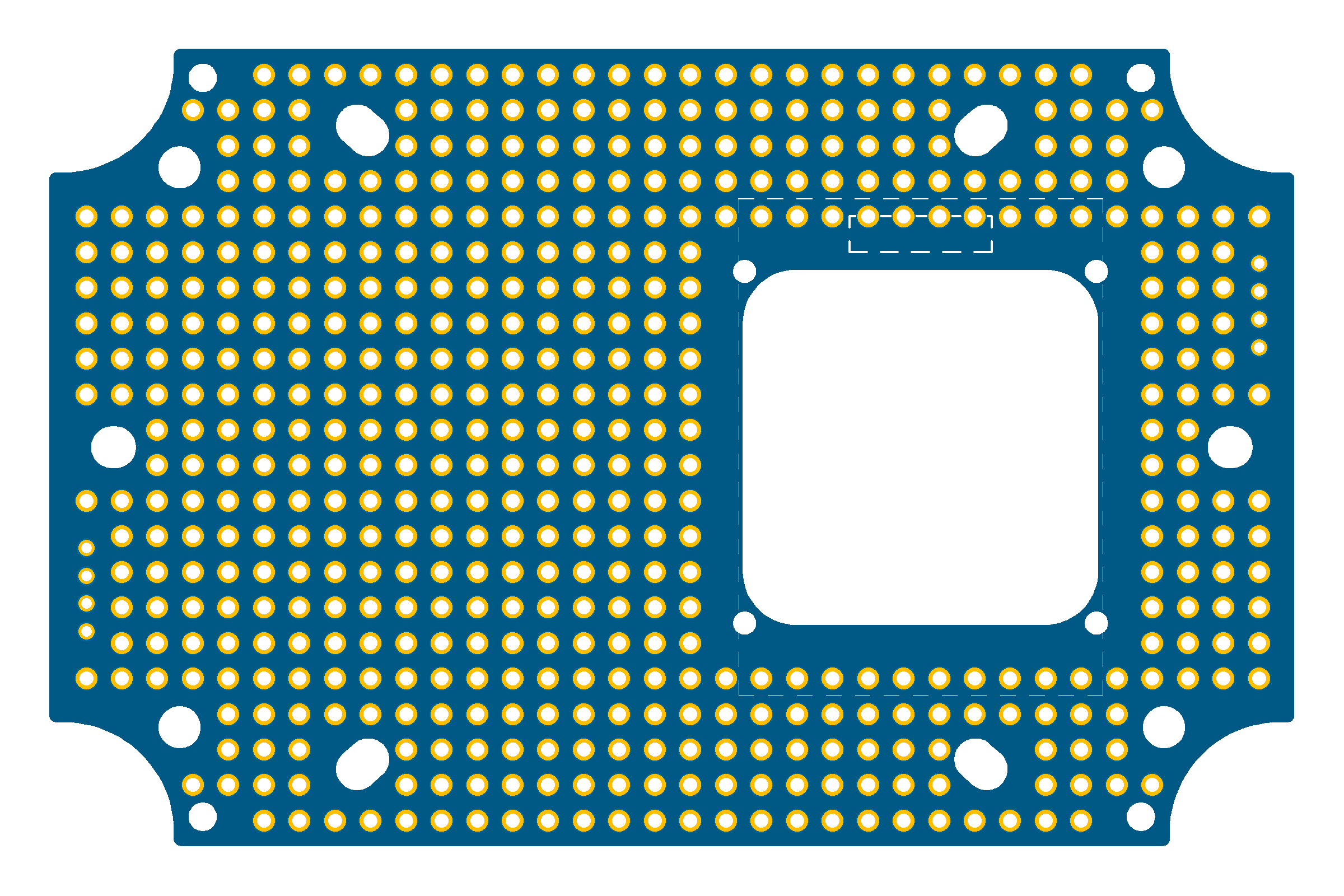 |
10068-GPSJ PCB
[10068-PDS] OLED Display/Sensor/Solar Panel Board
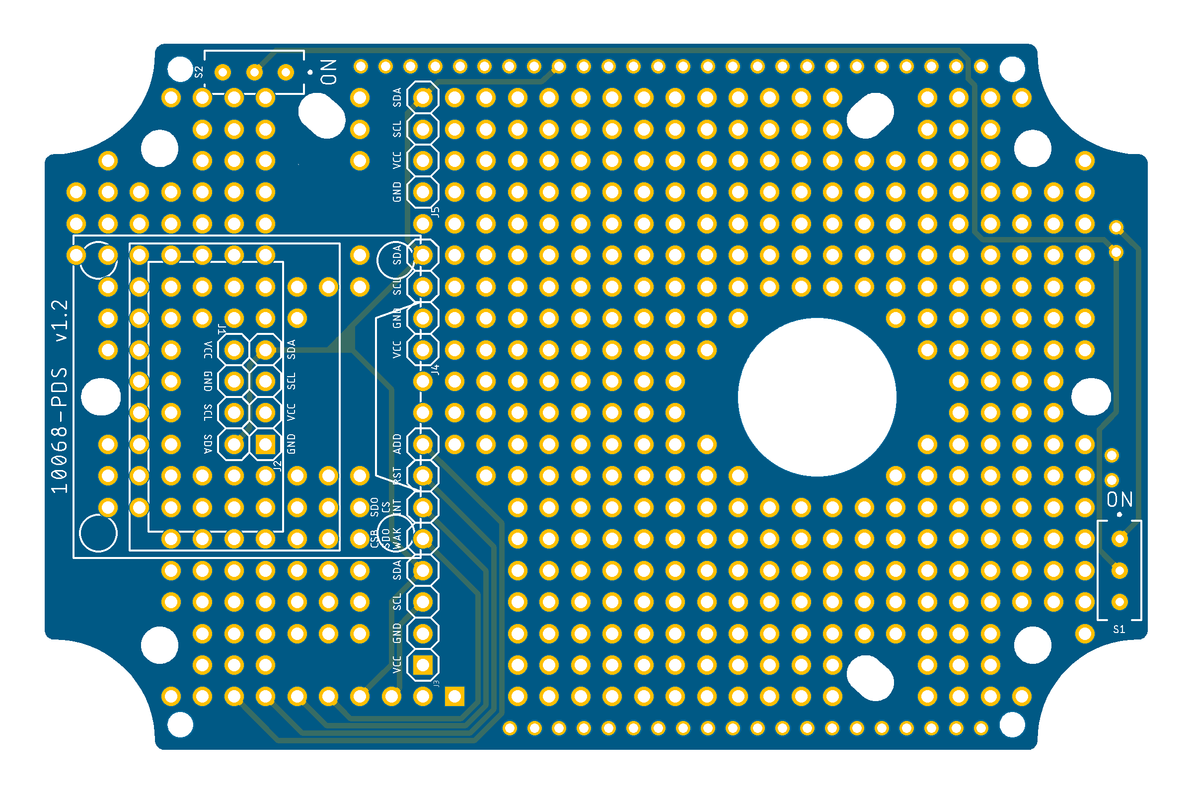
This board was specifically designed to provide a mounting point for an OLED display. In the process, however, it was easy enough to also include connectors for several sensors and a solar panel. Like the GPS Antenna Mount, the rest of the board incorporates a 100 mil pad array, but it also includes pads at 2 mm spacing along the edges for JST PH2.0 connectors. Like most of the other boards, this was designed to be used in conjunction with the BCS-A4a power board and associated processor, and as such includes standoff mount points common to all of the current 10068 boards.
Board schematic
| Top | Bottom |
 |
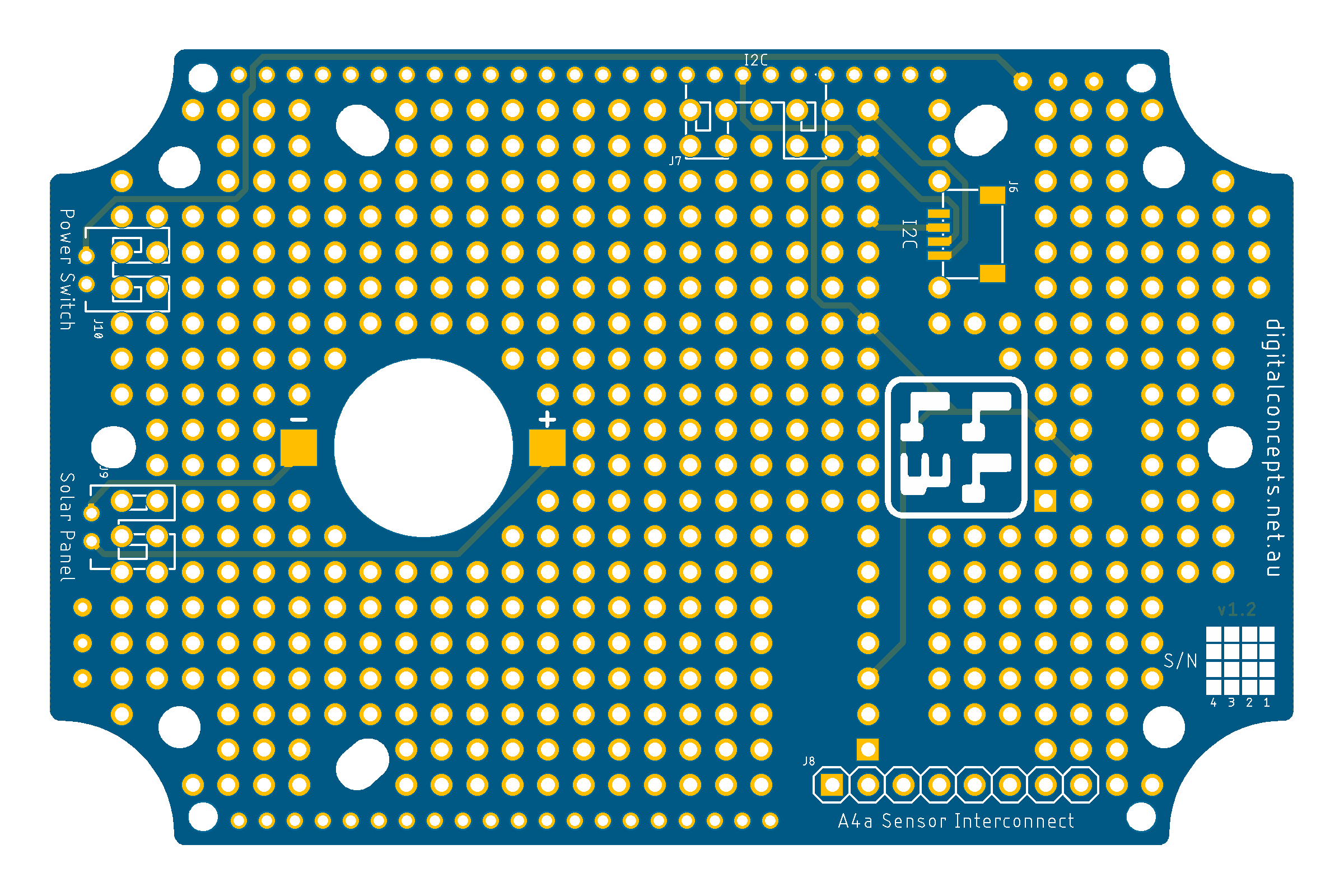 |
10068-PDS PCB
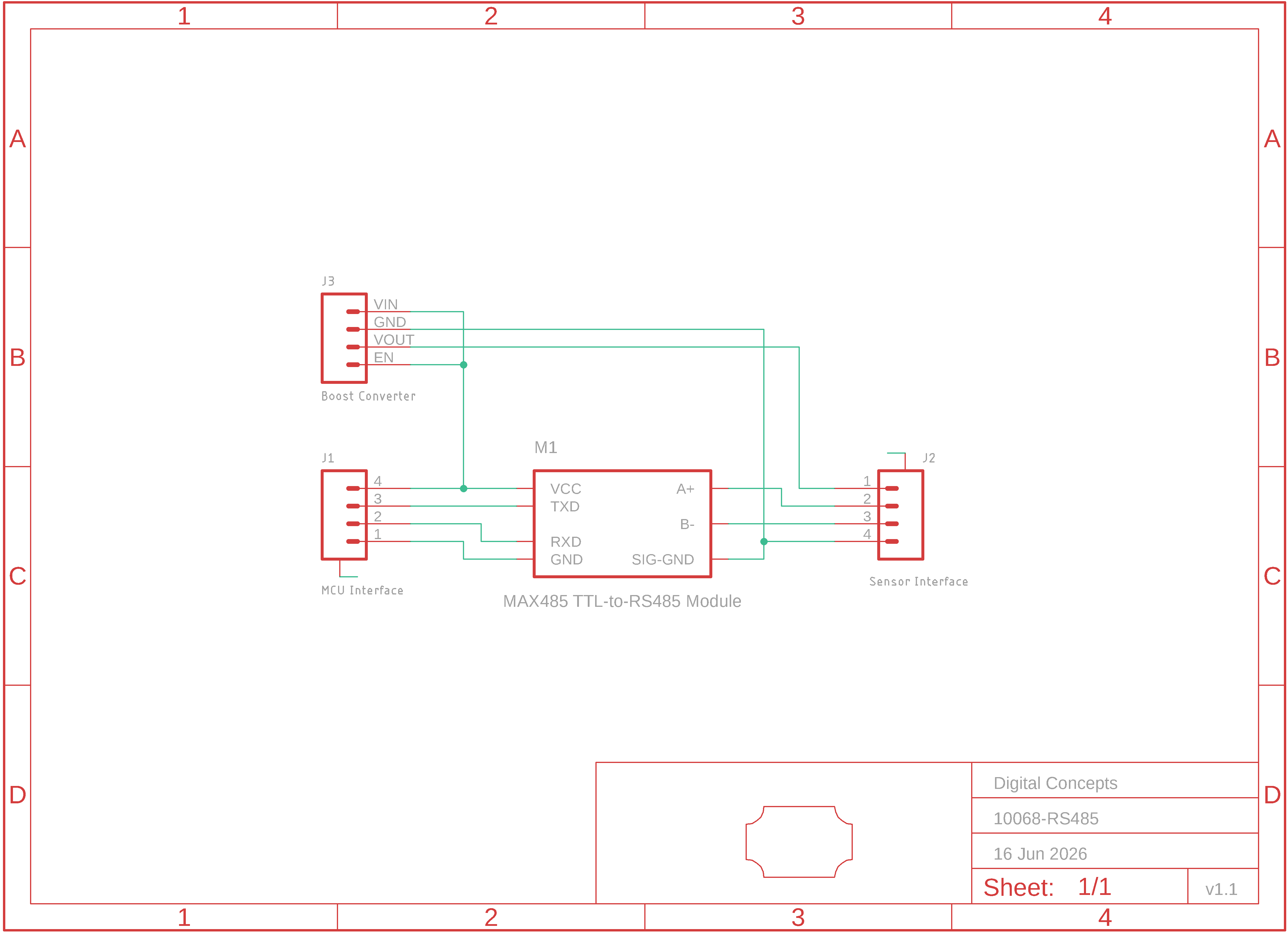
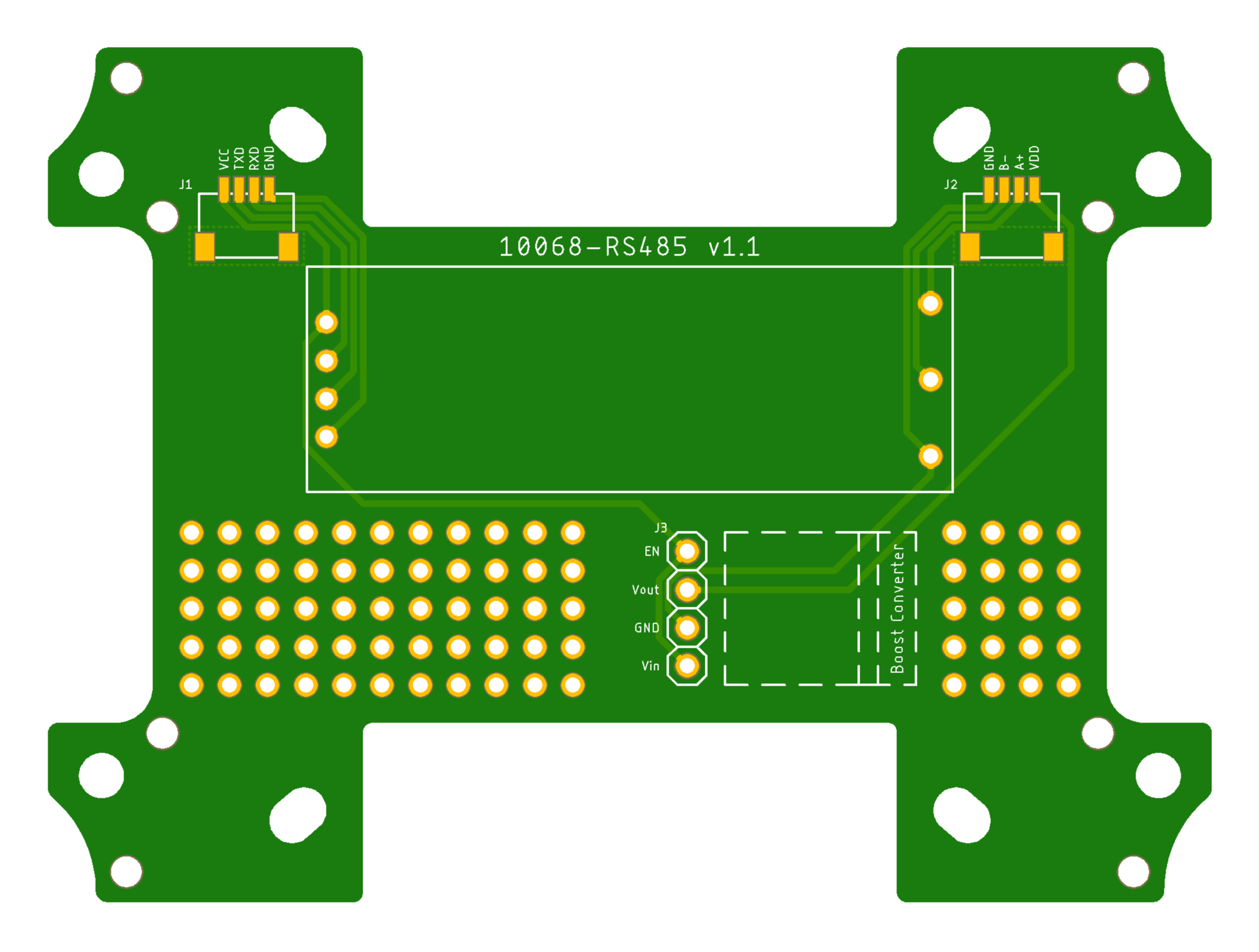
[10068-RS485] RS485 Board
Words...
| Top | Bottom |
 |
 |
10068-RS485 PCB
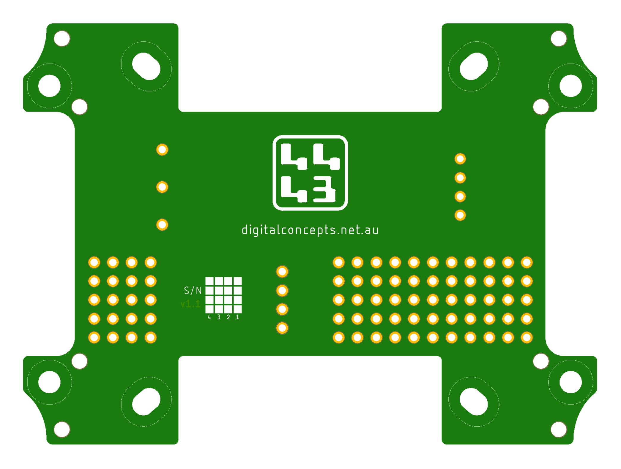
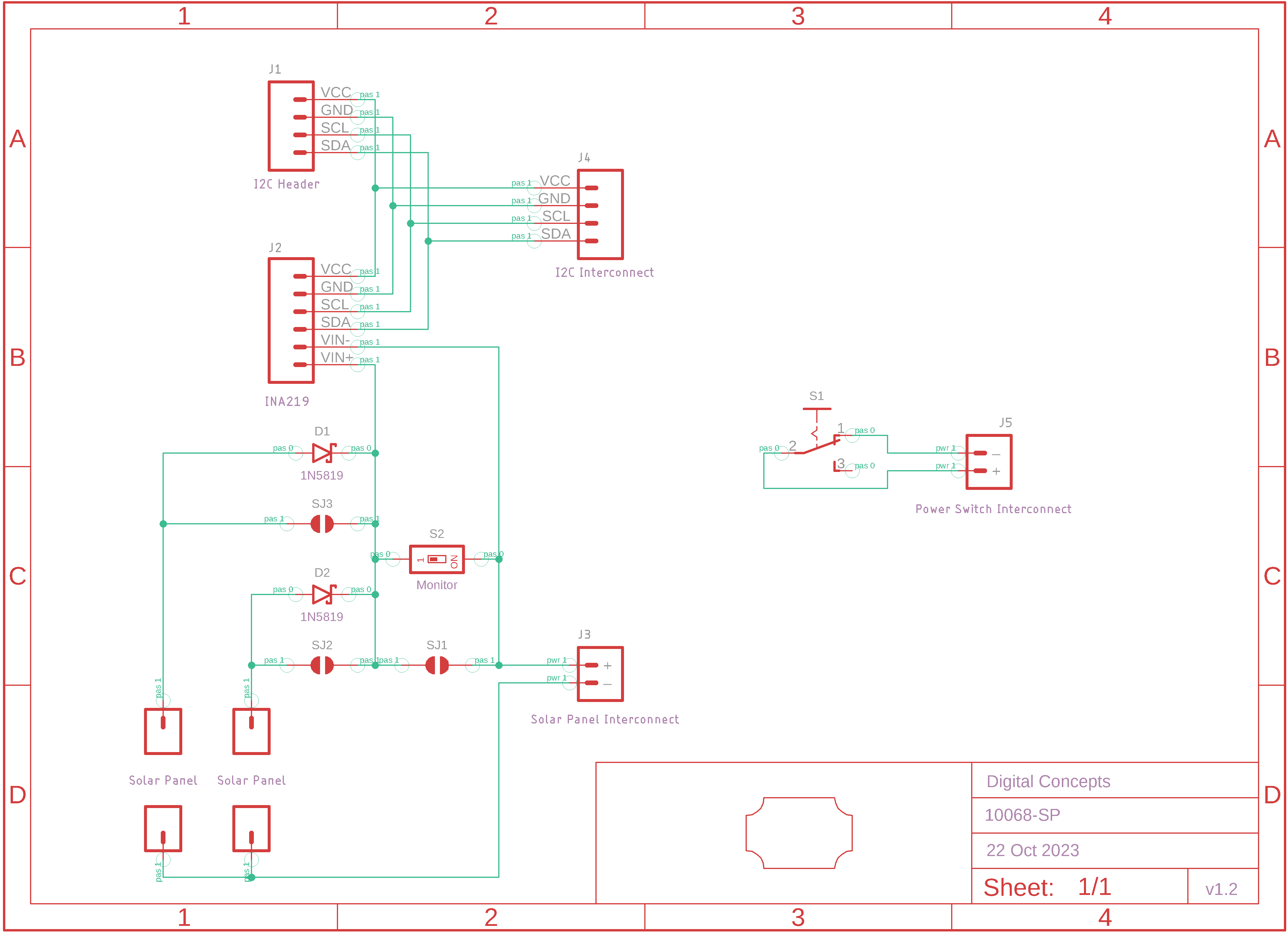
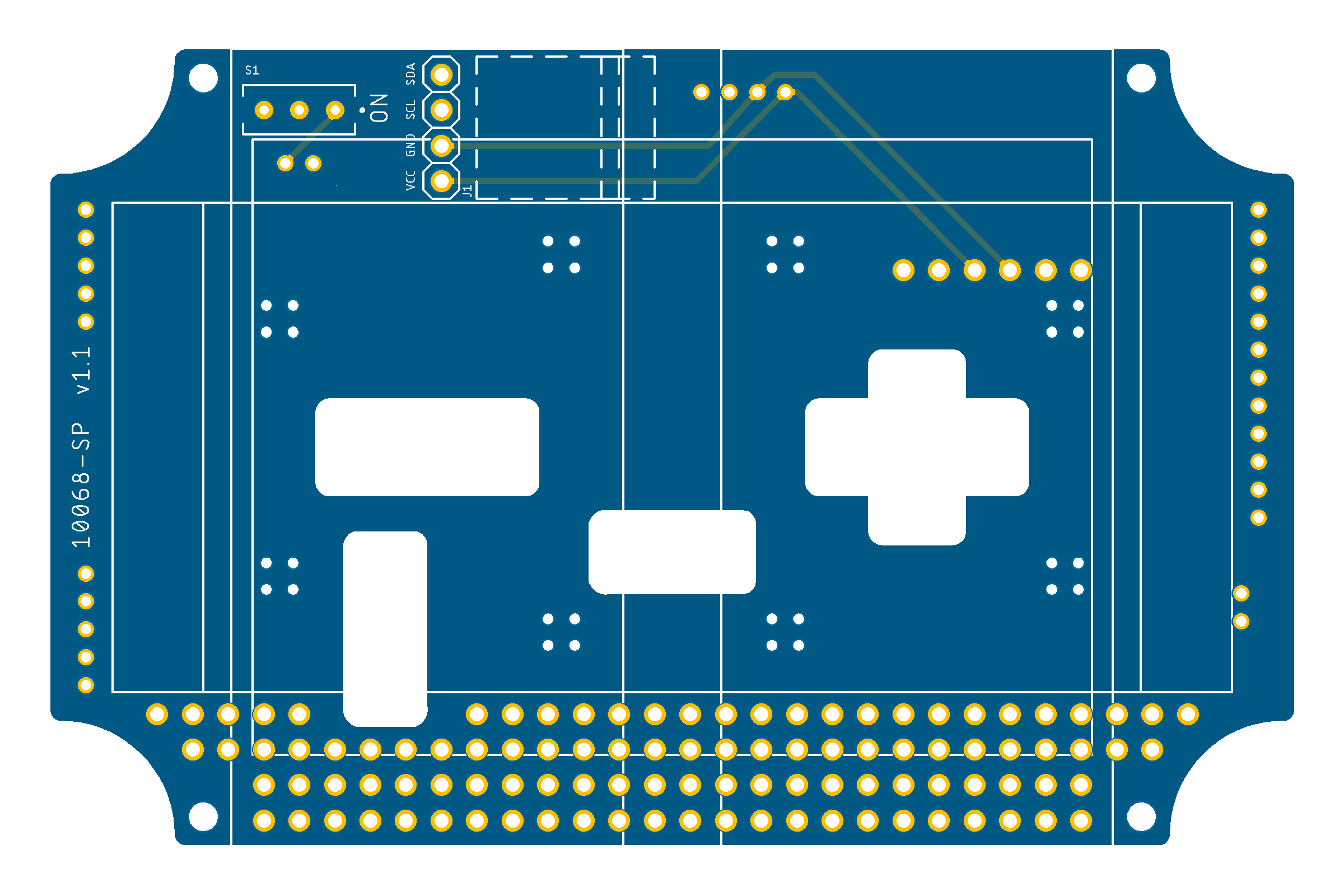
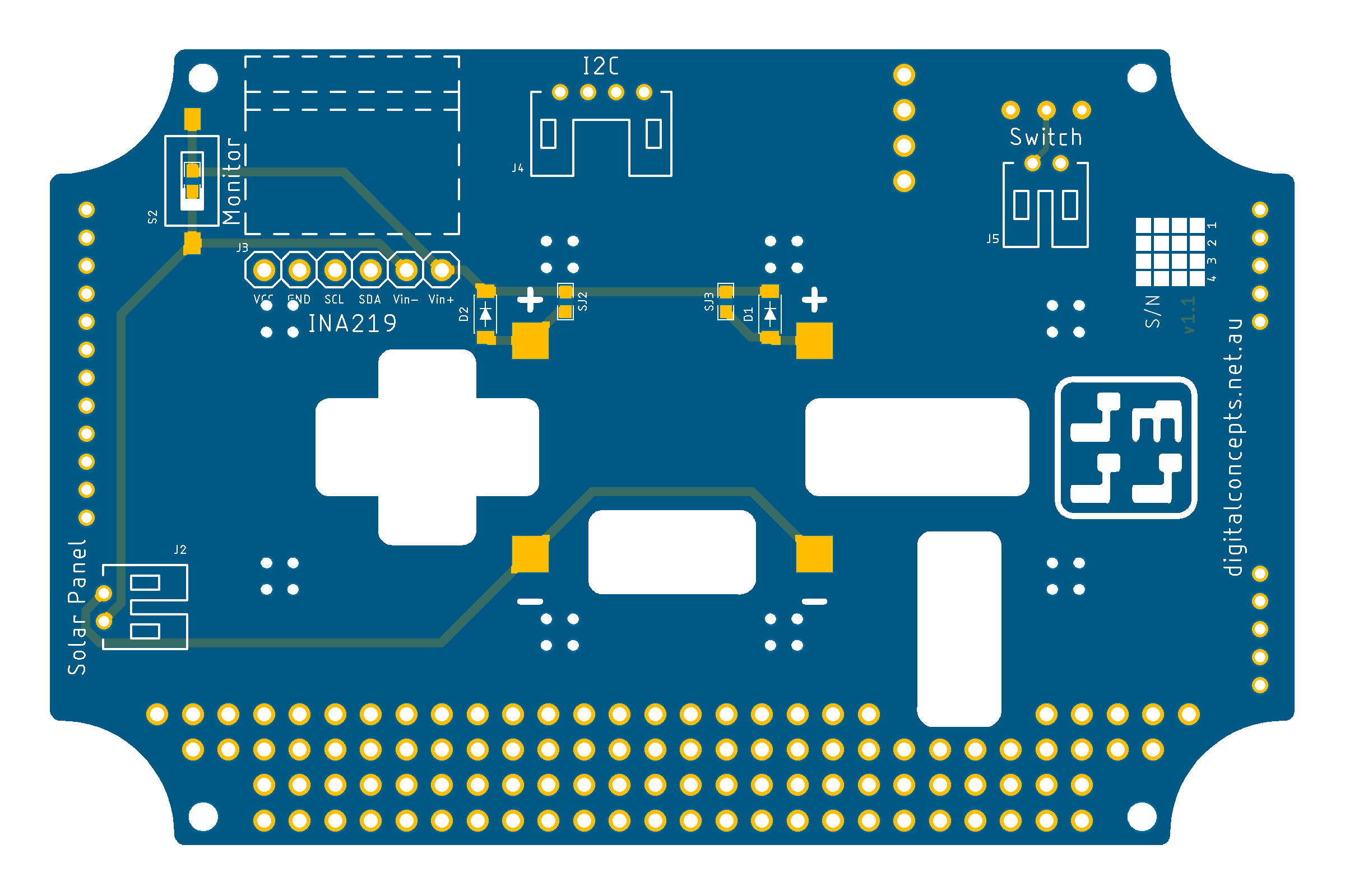
[10068-SP] Solar Panel Board
This board was designed to provide support for solar power input. The PCB is designed specifically for an 80 × 35 mm 5.5V 70mA solar panel, or up to two 57 × 28 mm 5.5V 40mA solar panels, but can support any panel that fits on the board (additional board features may be limited by the footprint of the solar panel(s) used). The board includes reverse current protection diodes and optional support for I2C modules, in particular MAX44009 ambient light sensor and INA219 current/voltage monitor modules.
| Top | Bottom |
 |
 |
10068-SP PCB
[10068-SR04] Ultrasonic Sensor Controller Support Board
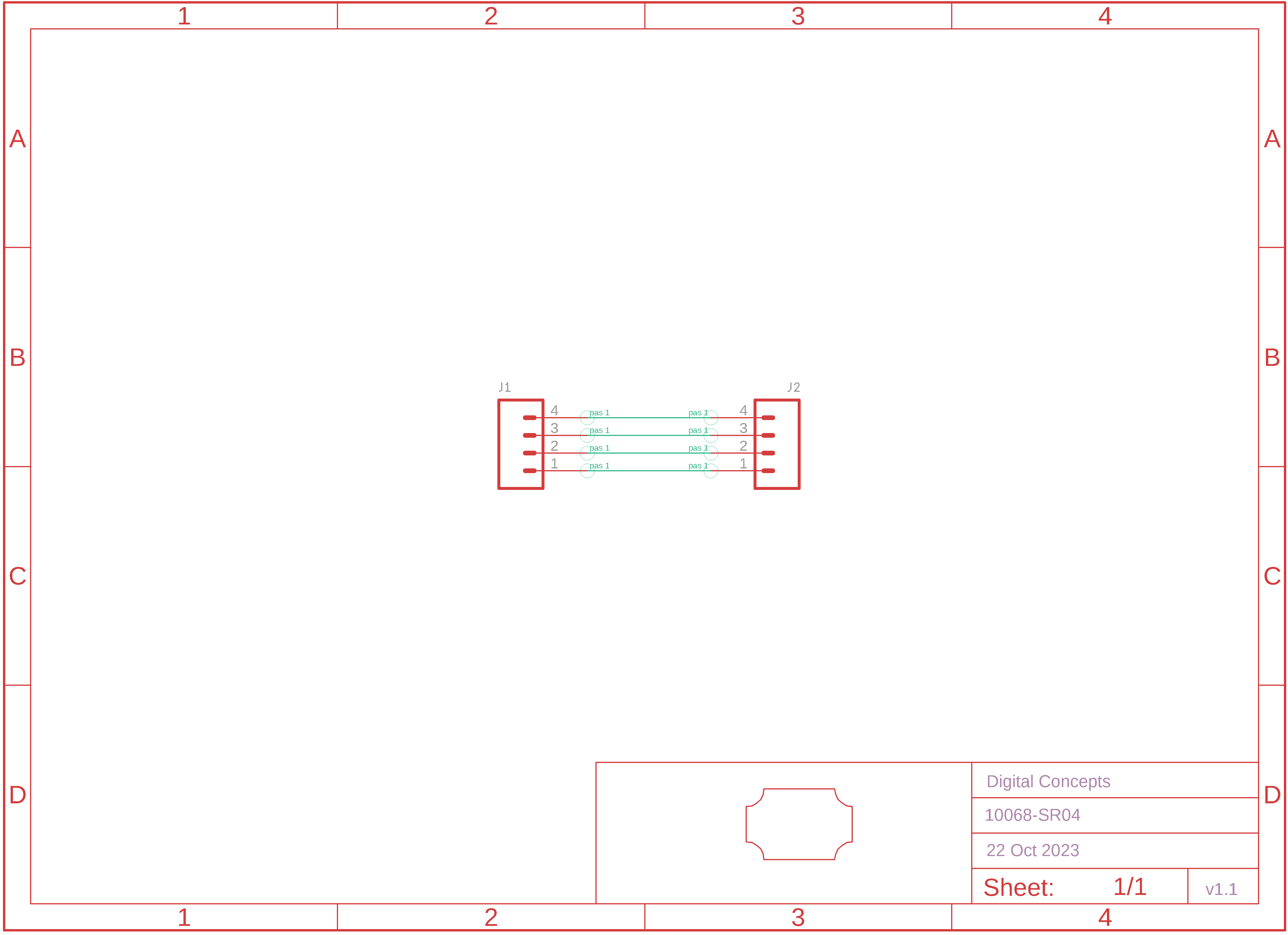
This board was designed to provide support for the controller board for an SR-04 ultrasonic sensor. The schematic in this case is trivial, simply specifying the connections between the pins of the header and JST connector.
| Top | Bottom |
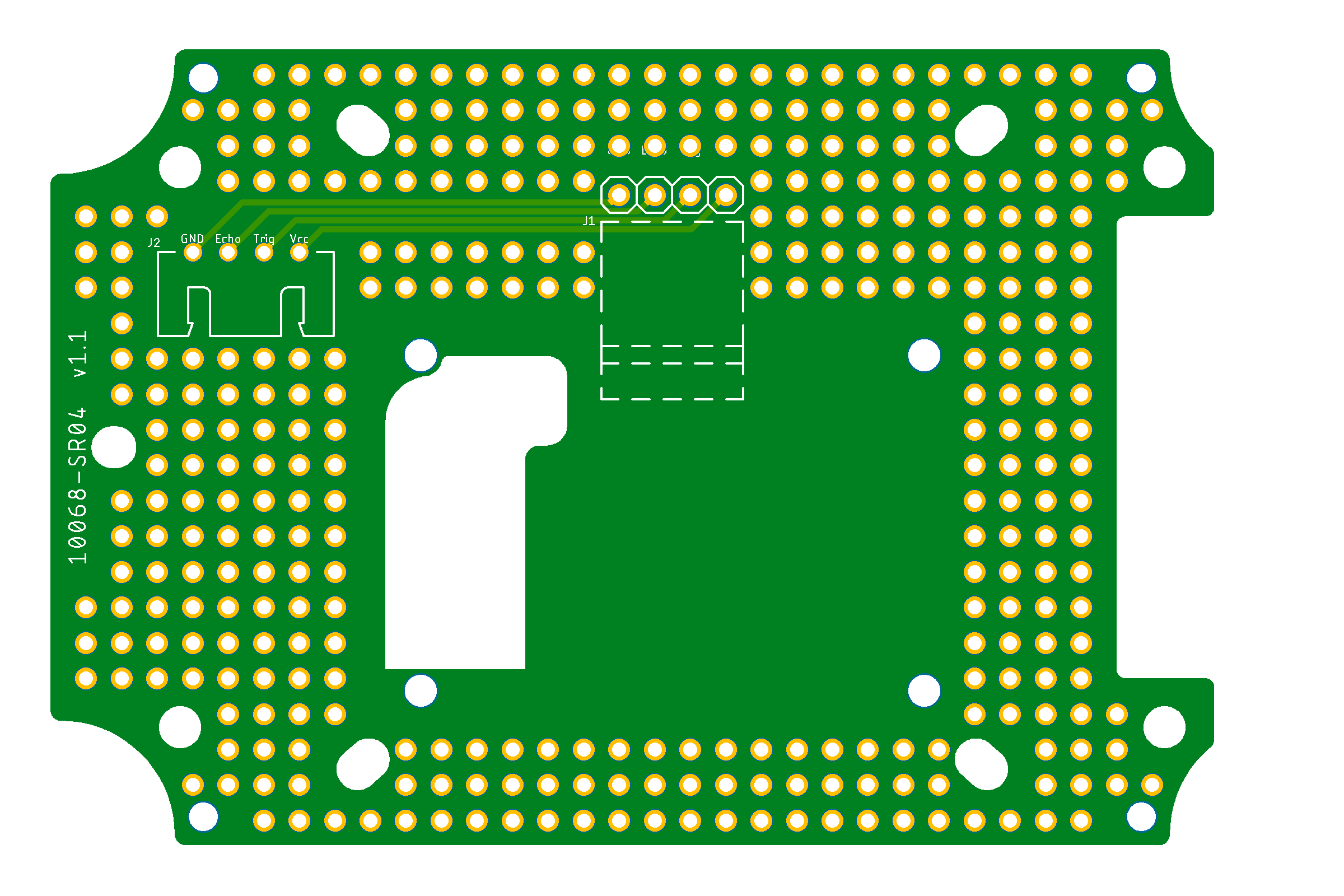 |
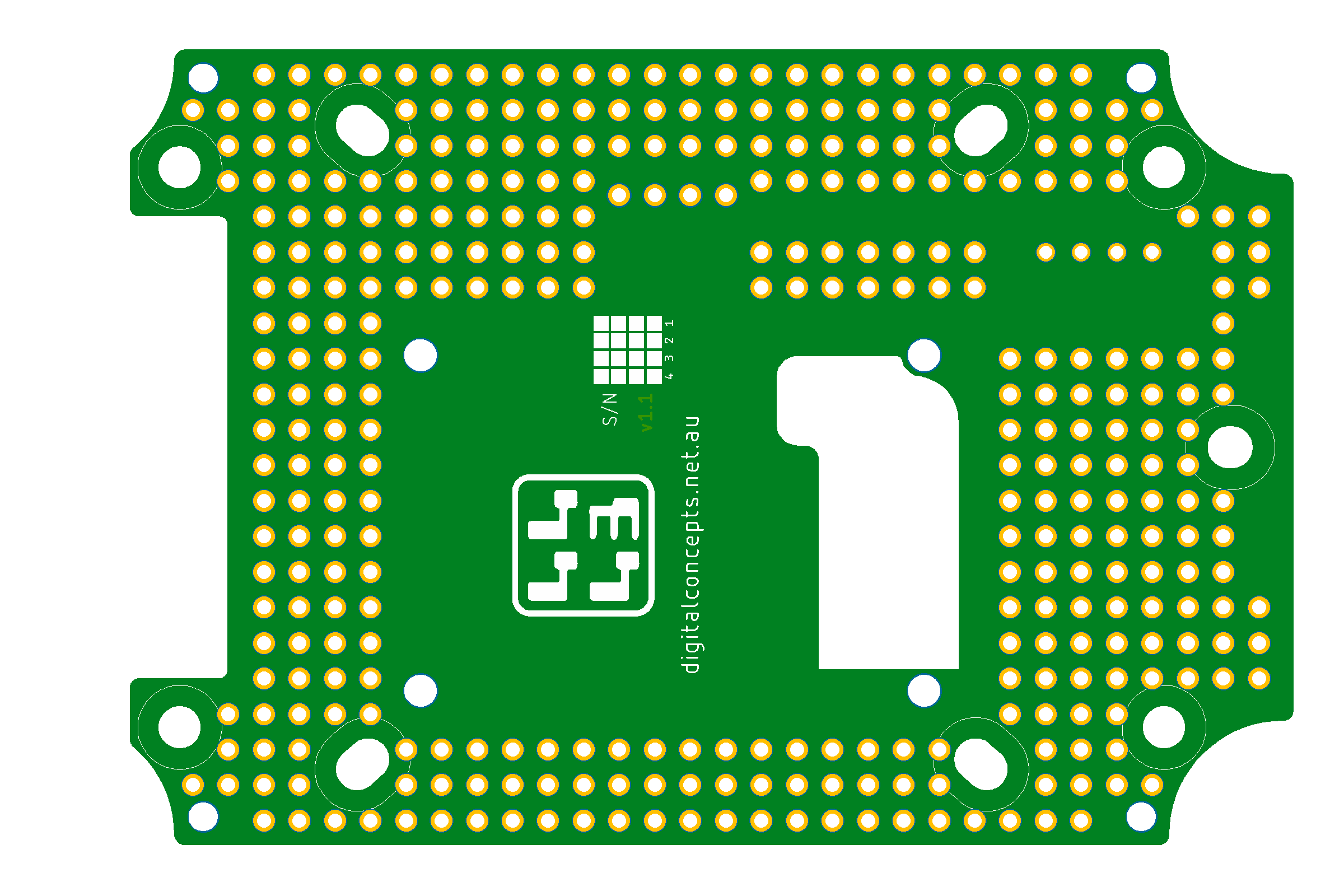 |
10068-SR04 PCB
[10068-WS] Weather Station Sensor Interface Board
This board was designed to provide a 'native' interface for weather station sensors, initially the RJ11 connectors used with the Davis 6466M rain collector (6P4C) and 6410 anemometer (6P6C). The board also includes RJ11 (6P4C), JST PH2.0 and 100 mil pin header interaces for I2C devices as well as spare RJ11 (6P4C) and JST PH2.0 connectors for any other 'single wire' sensor. Since weather sensors are often used in exposed locations, ESD protection circuitry is included on all sensor lines.
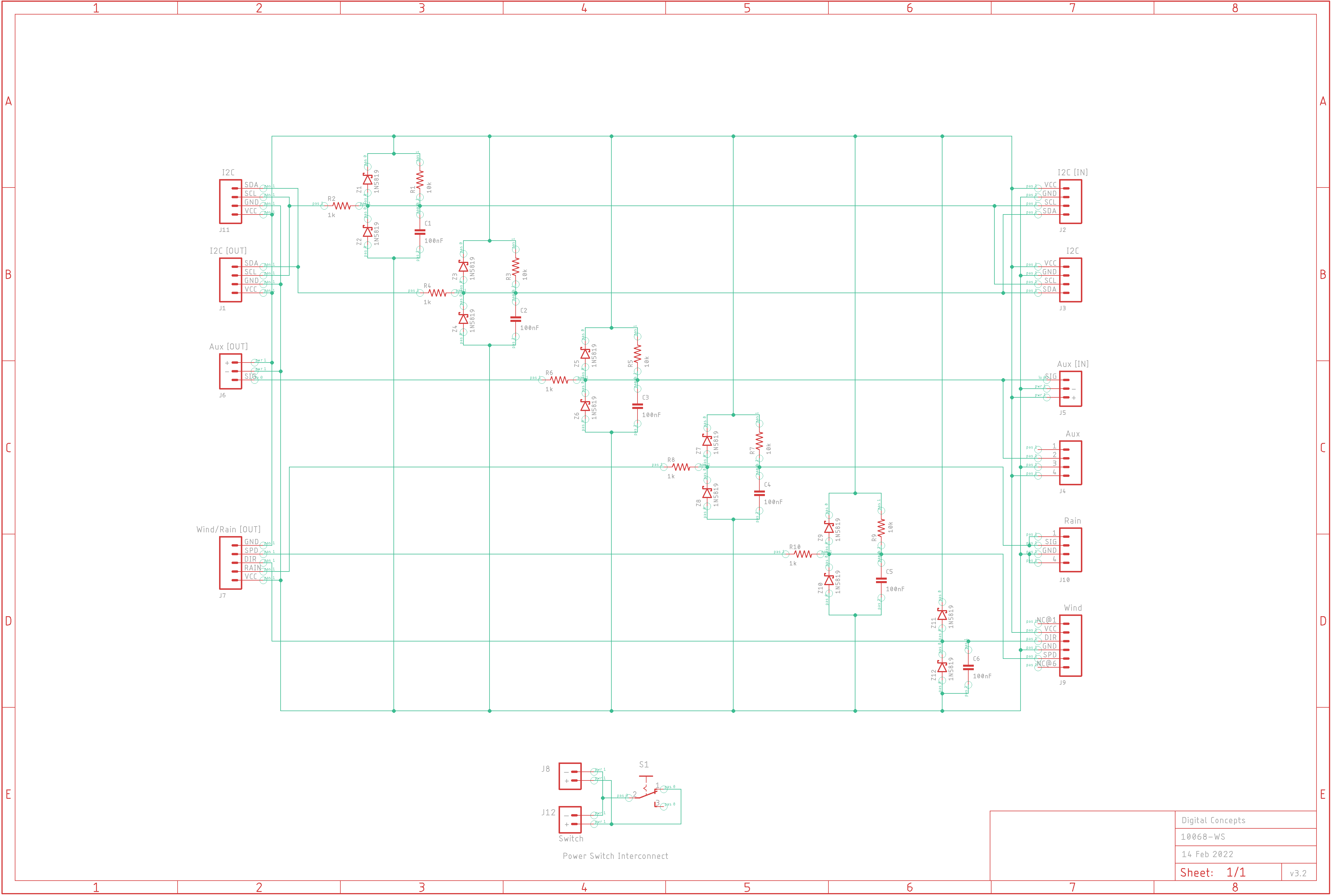
| Top | Bottom |
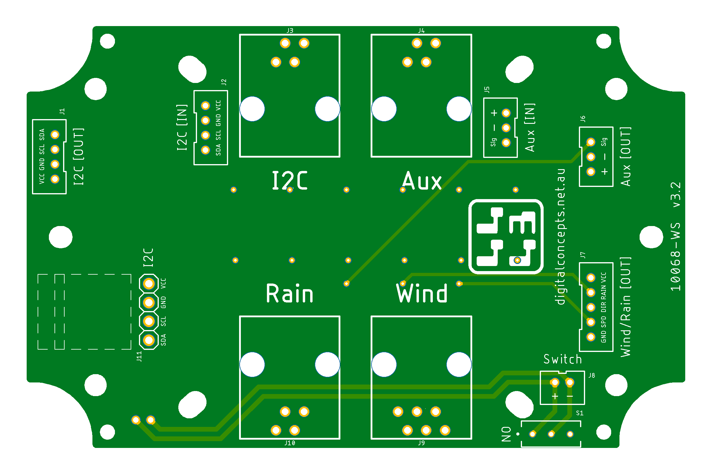 |
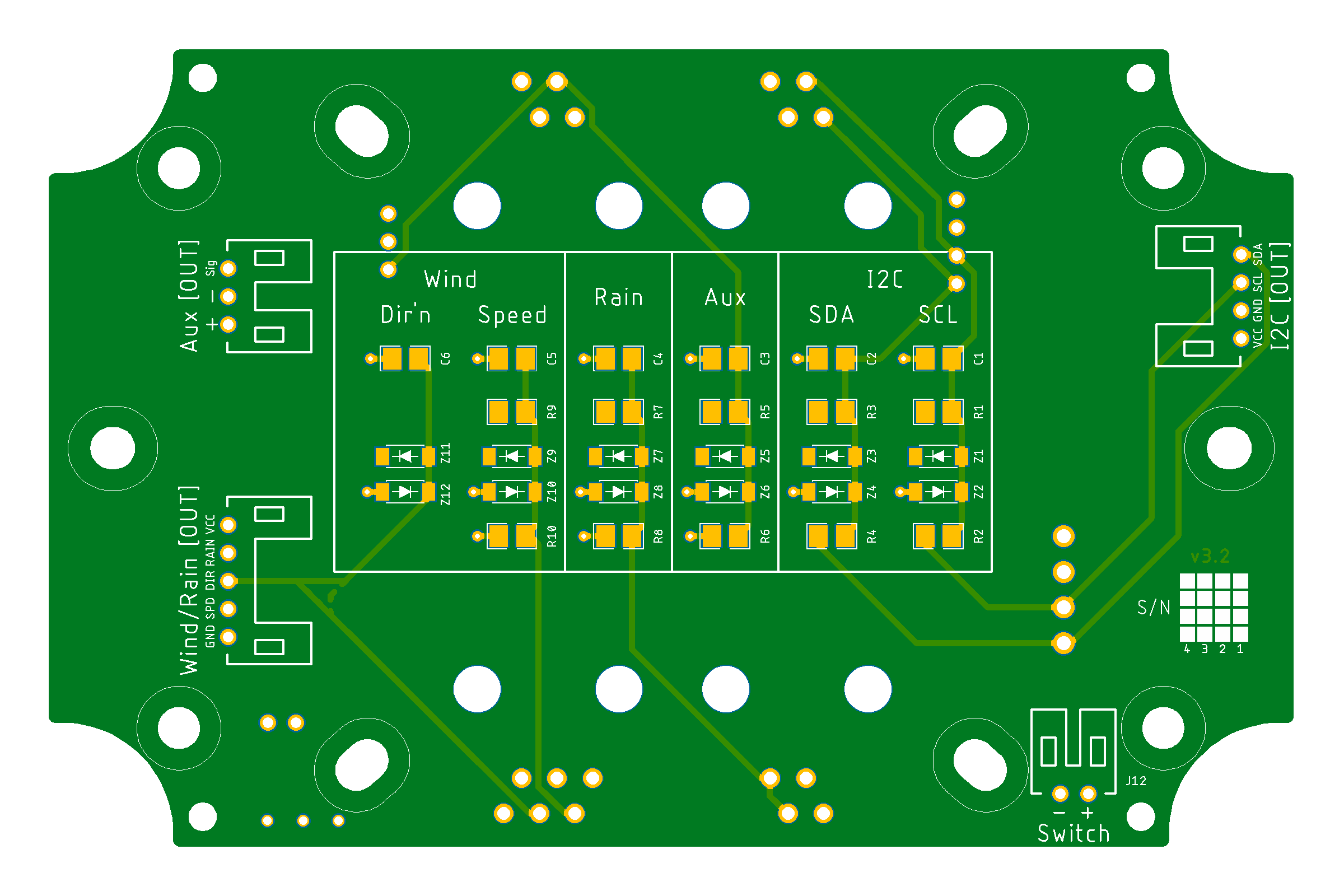 |
10068-WS PCB