10068-BCS-A4a PCB
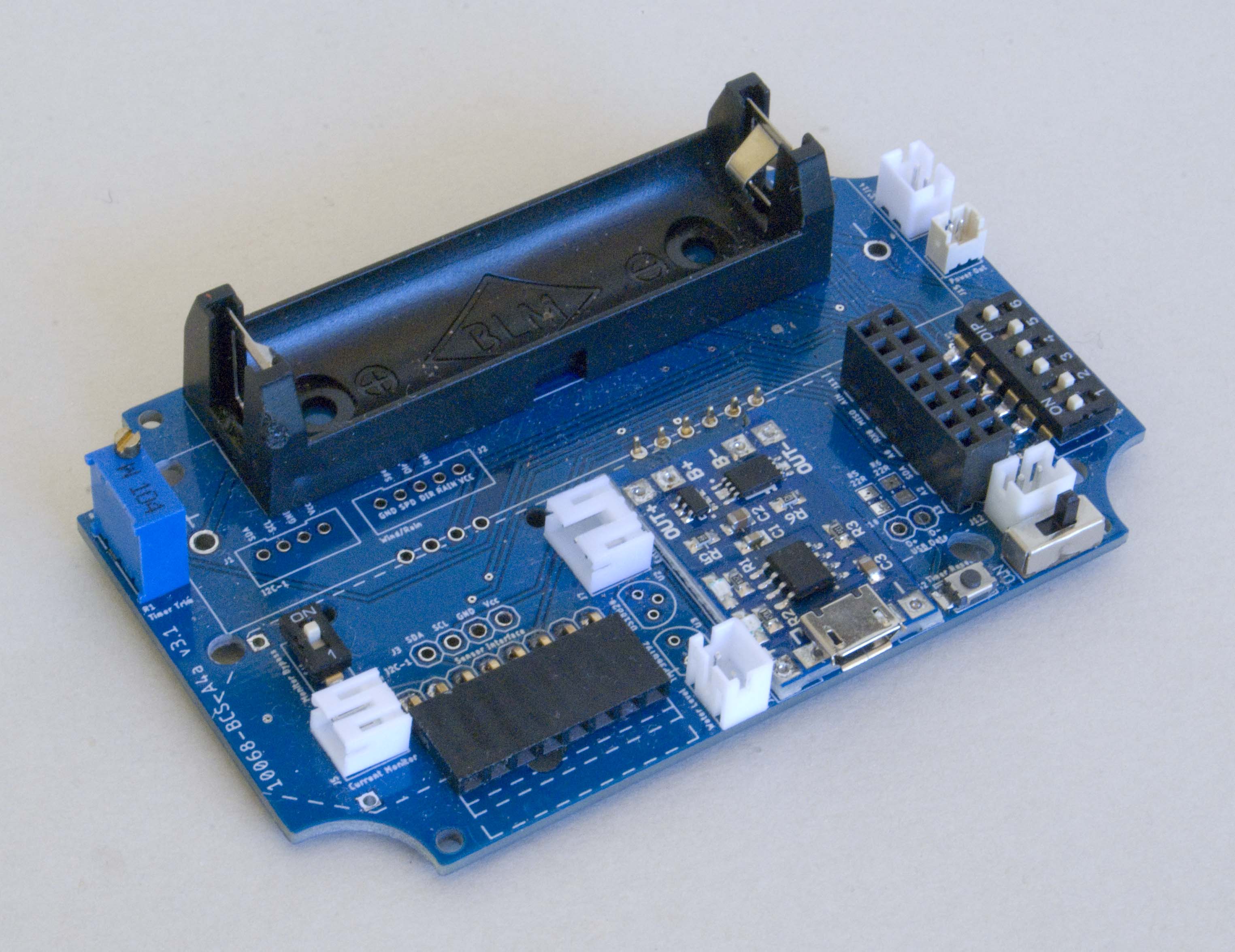
The BCS-A4a (Battery-Charge-Sensor with support for ALF4all processor daughter boards) boards (10068 and 8558) are prototyping boards designed as power provision and sensor support platforms for a range of processor modules that are connected through the 2 x 7 pin ALF4all 'Sandwich' interface, which breaks out SPI, I2C and serial Tx/Rx pins, as well as four (A0 – A3) control pins.
ALF4all Sandwich Interface Configuration
The present board form factor is specifically designed to be mounted within the larger of two readily available enclosures. As mentioned elsewhere, I began by just copying circuit features directly from the work of Charles-Henri Hallard and Wijnand Nijs. I started with the original ALF4all 'Sandwich' design because I thought it was neat, and it worked 'out of the box'. I then used that as a base to learn about PCB design and the whole world of electronics surrounding battery powered IoT nodes. The BCS-A4a boards were the initial result of these efforts and have been my primary prototyping boards, especially this one, the 10068-BCS-A4a, with DIP switches that allow the swapping of some components in and out of the circuit.
Board Layout
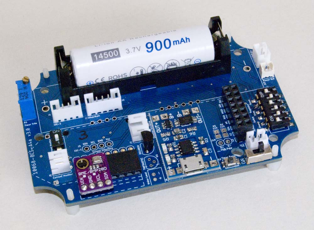
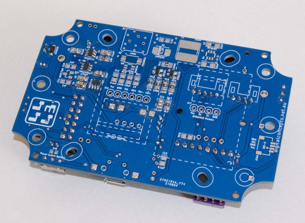
The various subsystems are identified in the board schematic and laid out as illustrated below:
| Top | Bottom |
|---|---|
 |
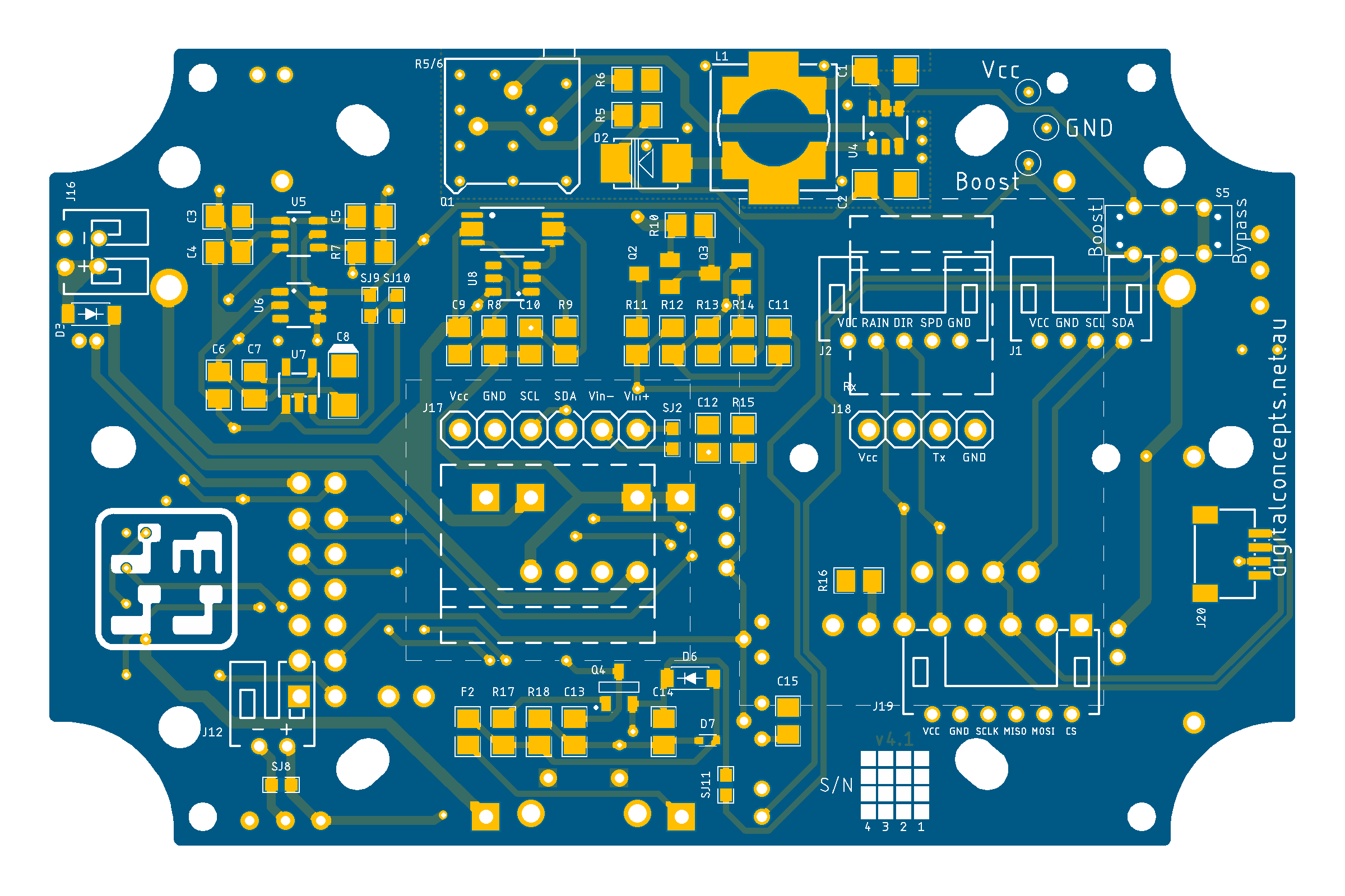 |
10068-BCS-A4a [v4.1] PCB
See here for CAD and CAM files.
Note: The current assembly instructions generally refer to the configuration and layout of the v3.1 PCB. The layout of later revisions of the board varies slightly, in particular, the main switch bank has only 5 DIP switches (the Boost Converter DIP switch has been removed). Where changes have any other practical impact, it will be noted.
Basic Configuration
The most basic configuration of this board requires little more than connecting a battery to a [ALF4all Sandwich] processor and required sensor interface(s). Solder Jumpers, or DIP switches, can be set to switch various board features in or out of a configuration. An optional master power switch can also be configured.
Battery Connection
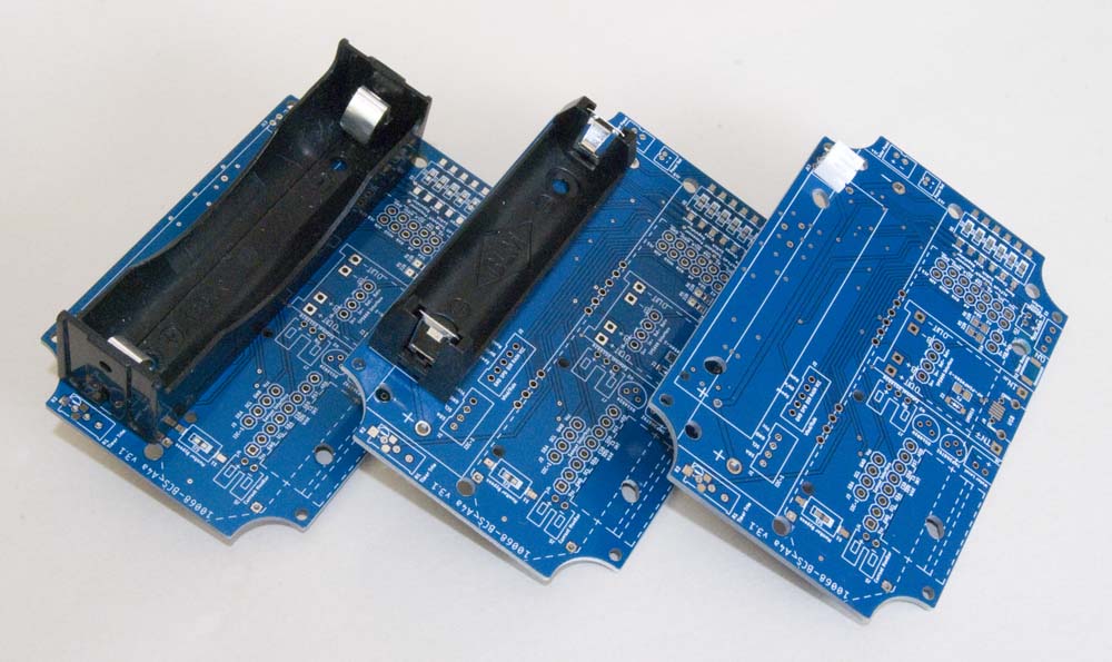
On the 10068-BCS-A4a PCB, pin locations are provided for 18650 (B1) and 14500 (B2) battery holders and a JST PH2.0 connector (J13) can be configured to support LiPo batteries. The smaller 8558-BCS-A4a PCB only supports the 14500 battery holder and the LiPo JST connector.
Battery Options
Solder Jumpers/Switches
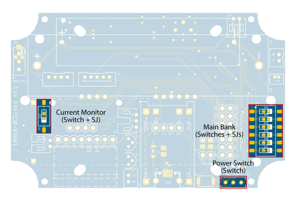
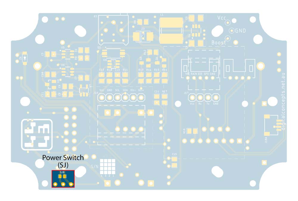
| Top (Switches + Solder Jumpers) | Bottom (Power Switch Solder Jumper) |
|---|---|
 |
 |
Solder Jumper/Switch Locations (v2.0 – v3.1)
| Top (Switches + Solder Jumpers) | Bottom (Switch + Solder Jumper) |
|---|---|
 |
 |
Solder Jumper/Switch Locations (v3.2 – )
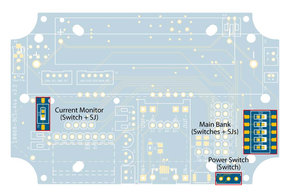
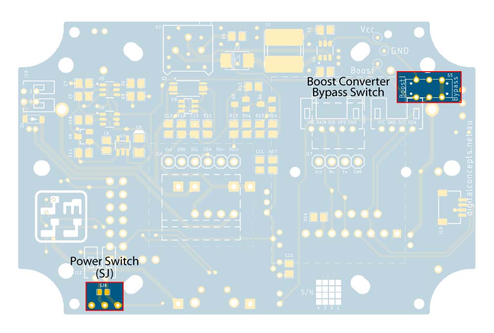
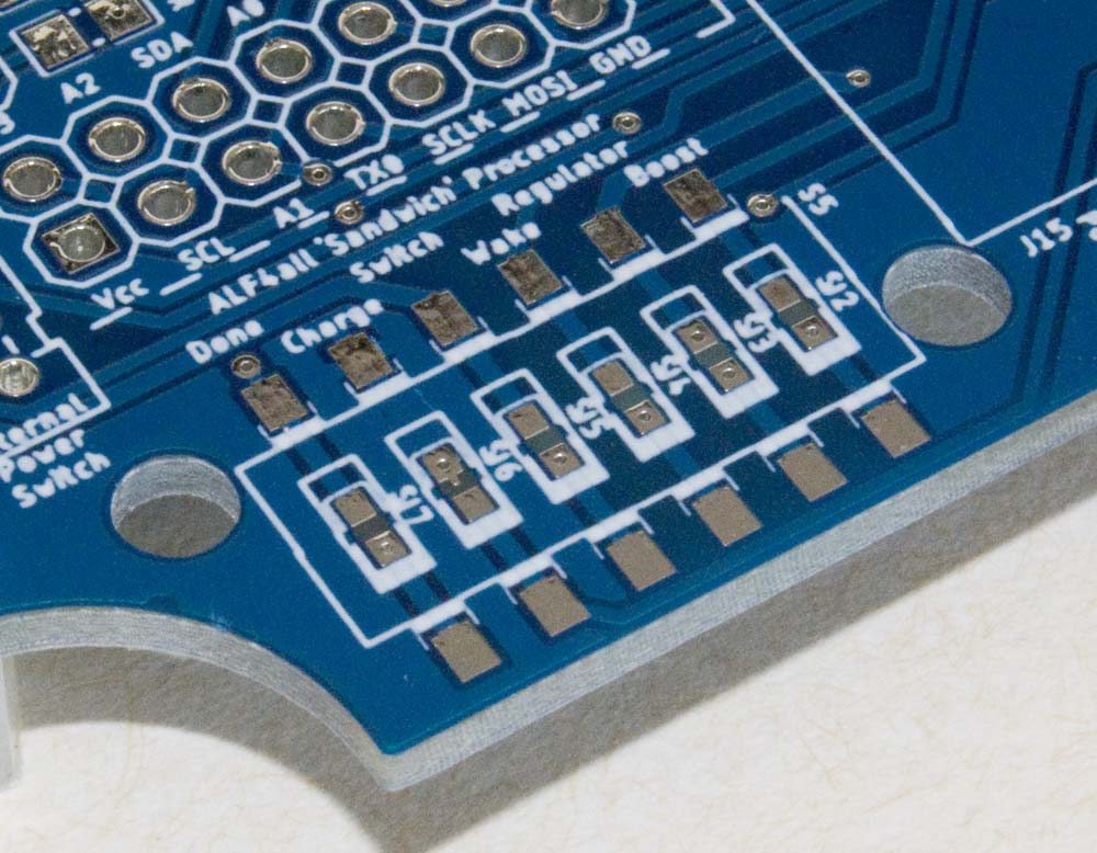
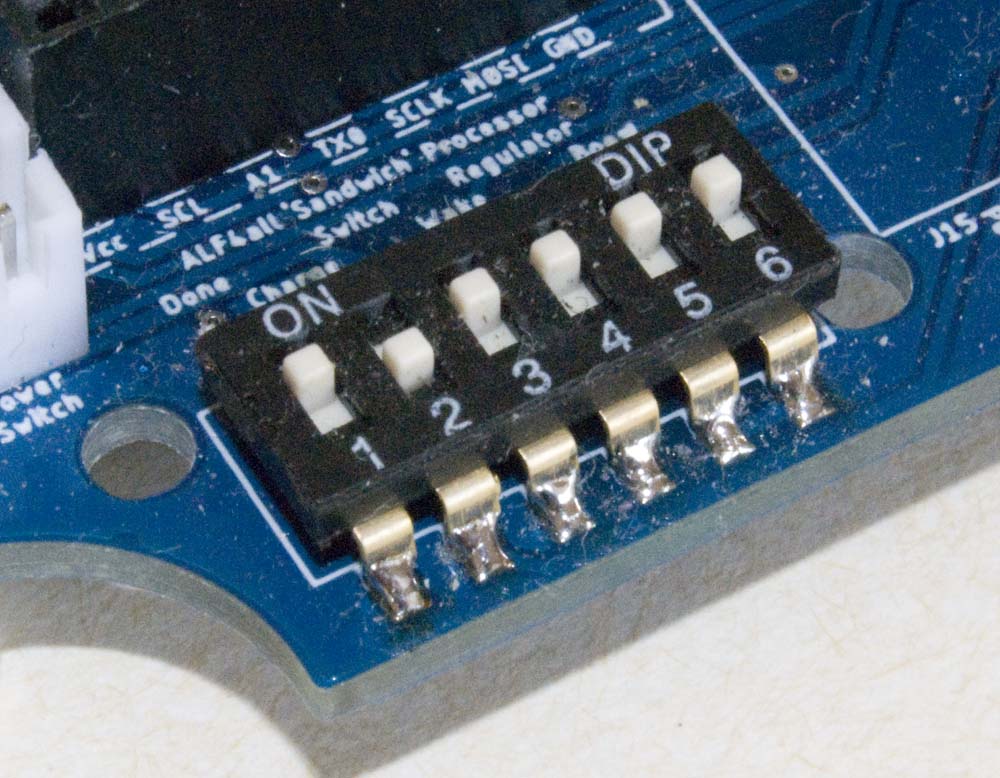
Most of the features on the BCS-A4a boards are optional. Originally, configuration of individual options required the bridging of associated solder jumpers. For prototyping work, however, it became convenient to be able to switch features in and out of the configuration, so I included a bank of DIP switches to handle most of the options. A power switch and a single DIP switch that can be used to switch a current monitor in and out of the power circuit are configured independently, along with their corresponding solder jumpers.
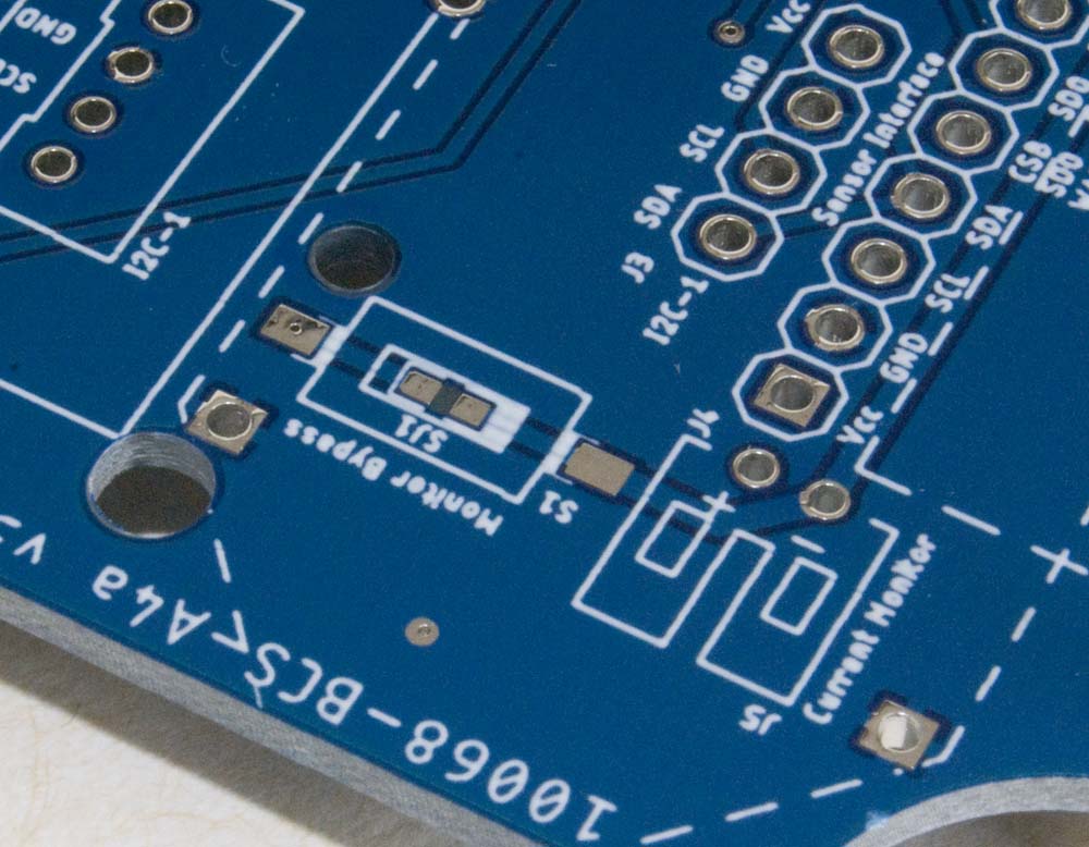
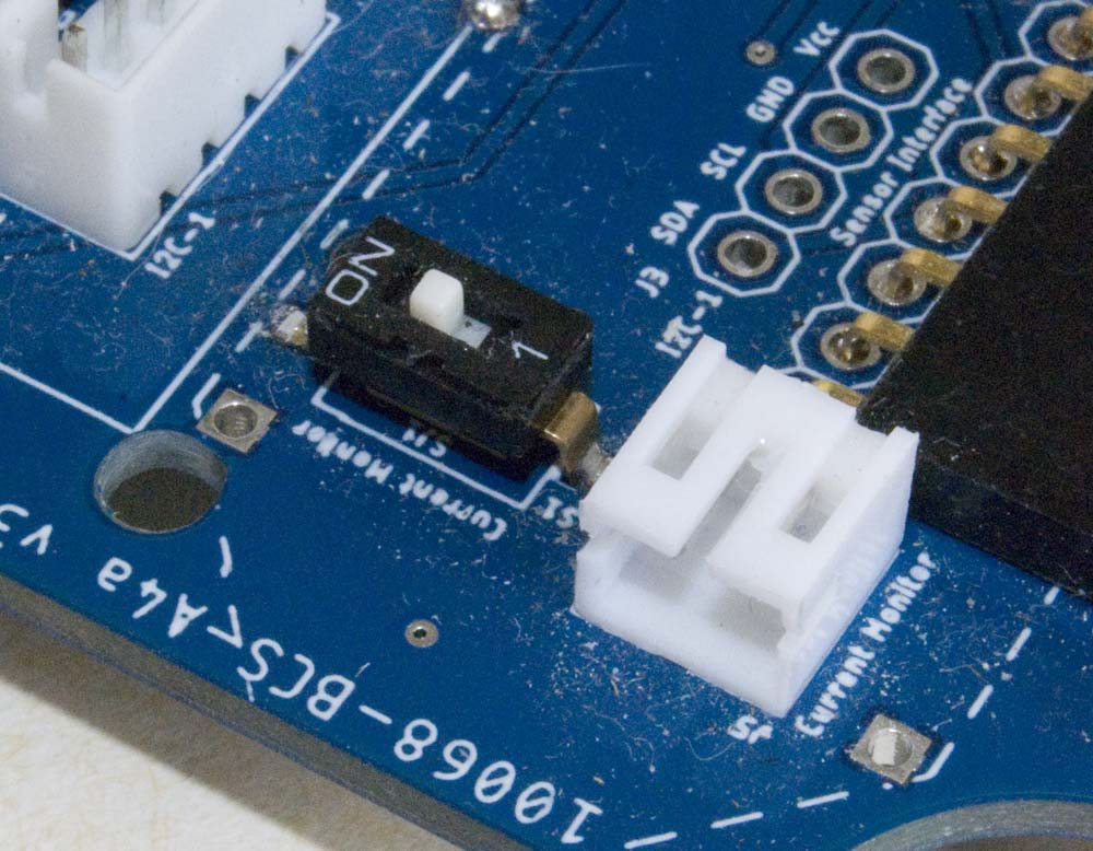
On the v2.0 and later boards, the solder jumper foot print is colocated with the corresponding [DIP] switch footprint so that it is covered by the relevant switch if the switch is installed.
| Solder Jumpers | [DIP] Switches | |
|---|---|---|
| Current Monitor (SJ1) |
 |
 |
| Main Bank (SJ2 – SJ7) (pre-v3.2) (SJ3 – SJ7) (v3.2+) |
 |
 |
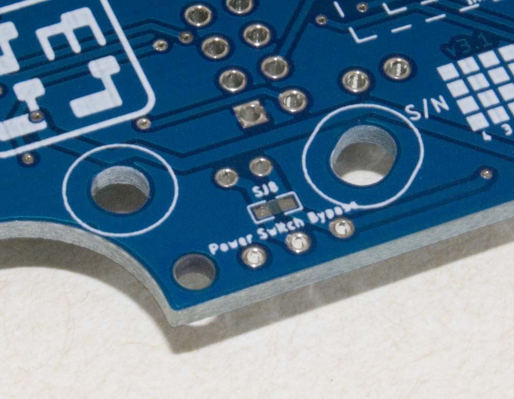
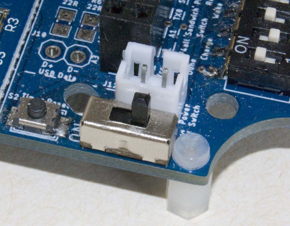
| Power Switch (SJ8) |
 |
 |
Solder Jumpers & Switches
Note: On v3.2 and later boards, there are only 5 DIP switches in the Main Bank—the boost converter bypass function is provided by a separate switch.
Solder Jumper/DIP Switch Functions
The functions of the seven DIP switches is listed in the following table. When a DIP switch is in the ON position, the listed function is active (e.g. when the Current Monitor DIP switch is ON, the Current Monitor circuit is bypassed), otherwise the listed function is inactive. A bridged solder jumper is equivalent to a DIP switch in the ON position.
DIP Switch Functions
| DIP Switch | Solder Jumper | Function |
|---|---|---|
| Current Monitor | SJ1 | Current Monitor Bypass |
| Main Bank 1 | SJ7 | A3 Circuit (DONE signal) |
| Main Bank 2 | SJ6 | Charge System Bypass |
| Main Bank 3 | SJ5 | TPS22860 Switch Bypass |
| Main Bank 4 | SJ4 | A1 Circuit (WAKE signal) |
| Main Bank 6 | SJ2 | Boost Converter Bypass (pre-v3.2 boards only) |
Power Switch
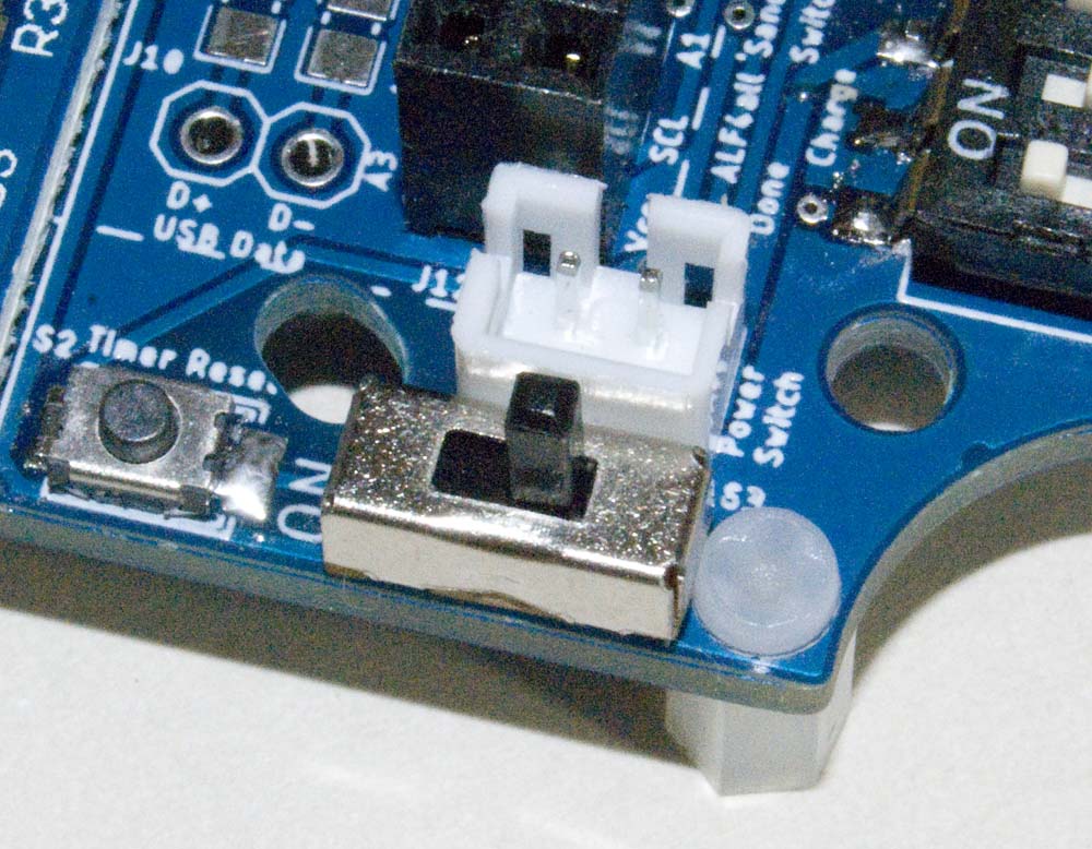
As noted above, power supply to the board can be configured permanently by bridging the solder jumper SJ8 or controlled via a switch (as illustrated).
Power Switch & Remote Power Switch Connector
A 2P JST PH2.0 connector can also be configured to allow connection to a power switch on a secondary board. While the board silkscreen locates this connector on the top of the board, the connector can actually be configured either vertically or horizontally on the bottom of the board. If installing on the bottom of the board, there is no silkscreen marking so consideration may need to be given to the polarity of the connector.
Configuration Options
 |
 |
Battery/Charge/Sensor Base Board
Apart from the various battery configurations, and the ALF4all 'Sandwich' processor interface, the boards can be configured with a range optional features:
- TP4056 or TP5000 battery charge management modules
- battery protection circuitry
- battery voltage and current monitoring circuitry
- solar panel input
- step-up boost converter
- low power/timer circuitry and voltage regulator
- timer reset button
- TMP35/36 analog temperature sensor
- DS18B20 digital temperature sensors
- HDL300 water pressure sensor
- I2C interface
- INA219 interface
- GPS interface
Battery Charging Circuit
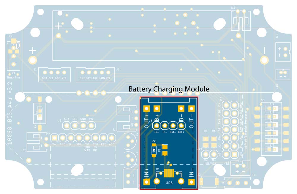 |
Battery Charging Module
I had originally intended to build my own 'on-board' charging circuit, using preconfigured modules just for prototyping and testing the performance of different options. As it is, for the time being at least, the modules are relatively cheap and don't take up much more room than the individual components, so this is as far as I've gone to date.
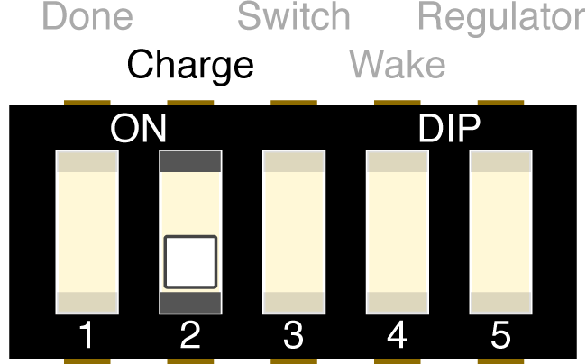
The battery charging circuit is configured into the system by default. The charging circuitry can be bypassed by bridging SJ3 or setting DIP switch 2 ON (if DIP switches are configured).
DIP Switch Setting – Battery Charging Circuit Active
To date I have used two different battery charging modules, one based on the TP4056 IC, for Li ion and LiPo batteries, and the other, primarily for LiFePO4 batteries, based on the TP5000 IC.
TP4056 Charge Management
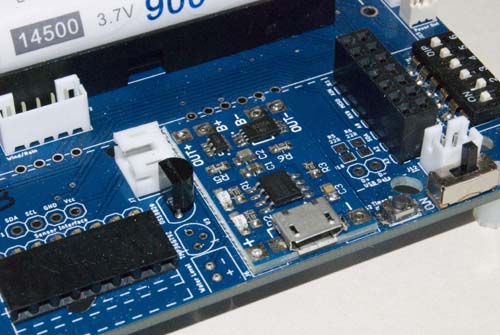
TP4056 Battery Charging Module
This is by far the simplest solution to on-board Li Ion battery charging—the modules cost ~A$0.30 in quantity. The TP4056 module (U3) I've used sits flat on my main PCB and comes with its own micro-USB Connector and on-board battery protection circuitry, so there are no other components required. There's no need to use headers to connect it to the main PCB. I just put a small amount of solder paste on each pad, sit the module in place, then heat up each pad in turn to melt the paste. I then usually follow up by filling each of the six pad holes with solder.
TP5000 Charge Management
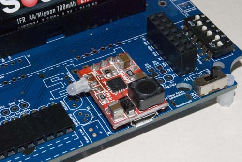
TP5000 Battery Charging Module
Using the TP5000 charging module (connected via header J5) is a little more fiddly, but it includes support for LiFePO4 batteries, which require a lower charging voltage than Li-Ion ones.
The module used here (there are others, some based on the CN3801 IC for example, that also support the LiFePO4 chemistry) is more basic than the TP4056 module in that it does not include a USB interface or any battery protection circuitry. Both of these, however, USB power input and battery protection circuitry, are provided as configuration options on the present BCS-A4a boards.
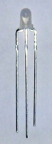
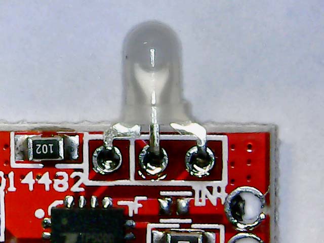
The common cathode bi-colour LED that was supplied with the first modules I purchased was actually the wrong LED. A common anode bi-colour LED is what is required, so it's worth checking before soldering the LED in place. More recent items I have purchased have indeed been supplied with either a common anode red/blue or red/green bi-colour LED, which should be installed as illustrated below (Note: longer red leg on the left, with the square connection to the LED head, shorter blue or green leg on the right, with the rounded connection to the LED head):
| LED Leads | LED Orientation |
|---|---|
 |
 |
TP5000 Bi-colour Status LED
When installed in this orientation, the LED will light red when charging and blue or green when in standby mode.
A comprehensive review of the TP5000 module that I used is provided here.
micro-USB Connector
 |
USB Connection
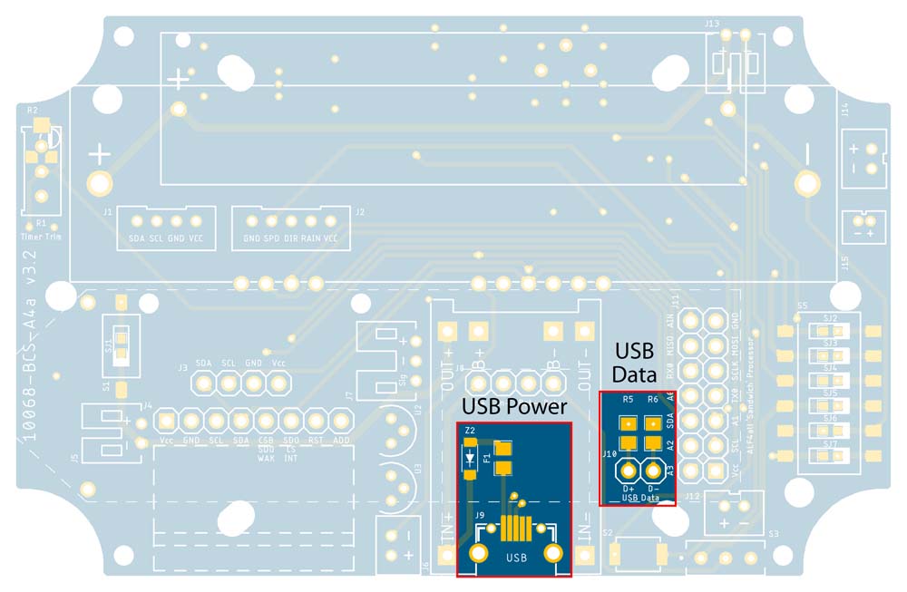
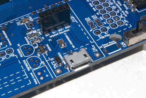
The USB connector (J9) is provided as an additional charging source when using the TP5000 battery charge management module. It is configured with an MF-PSMF050X-2 resettable fuse (F1) and 1N5819 Schottky diode (Z2) to protect against over-current conditions. The data pins are also broken out from the USB connector, but are not currently used in any of my applications.
 |
 |
micro-USB Connector
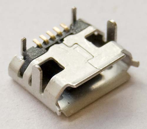
There are many different micro-USB connectors available and I abandoned the idea of attempting to accommodate different connectors early on. If you have a different USB connector to the one illustrated, you will need to modify the PCB footprint accordingly.
Battery Protection Circuitry
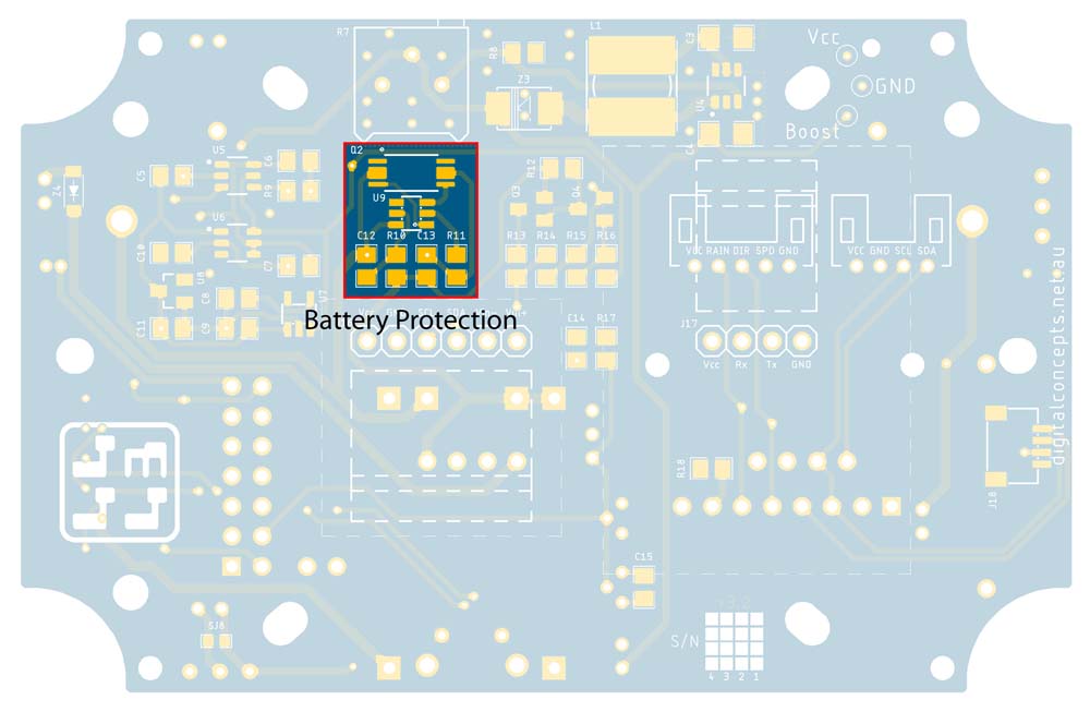 |
Battery Protection Components
These elements are not required for the TP4056 module used here, as it includes its own protection circuitry.
If using the TP5000 battery charge management module (generally only required if using LiFePO4 battery technology) configure U4 (FS8205A), Q1 (DW01A), C12 (10µF), C13 (100nF), R10 (100Ω), R11 (1kΩ). This is the same circuitry that is included on the TP4056 module.
Battery Voltage Monitor
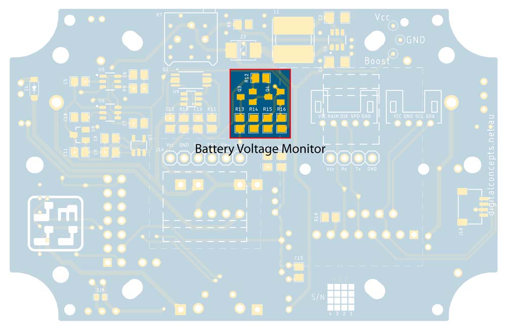 |
Battery Voltage Monitor Components
Used to monitor battery voltage, this is effectively a voltage divider that is controlled by a pair of MOSFETs—BSS84 (Q3) & BSS123 (Q4)—so that it can be switched on only when required, avoiding the quiescent current leakage normally associated with an active voltage divider. I essentially copied this circuit from the IoT Battery/Sensor board developed by Wijnand Nijs and the battery level monitor developed by Oliver Hanka.
When there is a battery in the circuit, the 100kΩ pull-up resistor keeps the P-channel MOSFET (BSS84) OFF. A LOW signal is then required on the gate to turn this MOSFET ON and activate the voltage divider. Since we need everything to be OFF when the processor is idle (pins floating/LOW), and only active when the processor sets a pin HIGH, we need another switch to activate the circuit when the processor sets a pin HIGH. The N-channel MOSFET (BSS123) does just this, switching ON when its gate voltage (A4a Sandwich pin A2) is HIGH, pulling the gate voltage of the P-channel MOSFET LOW and activating the voltage divider. The voltage in the circuit can then be measured through A4a Sandwich [analog] pin A0.
Some processors seems to have a more stable ADC than others. The ESP32, in particular, does not have a very good reputation for consistency. I found that inclusion of the capacitor specified in the Hanka circuit improved the consistency of readings in this case (refer to the Software section for more specific details of measurement techniques).
The voltage monitor circuit can simply be omitted if not required.
Current Monitor
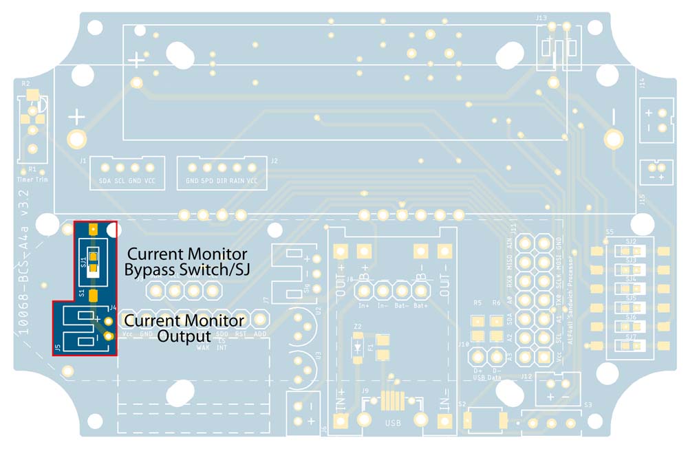 |
 |
Circuit Current Monitor JST Connector & Bypass Switch
The 2P JST PH2.0 Connector (J5) provides a connection point for an external current monitoring device. I typically use a Nordic Power Profiler Kit II for this purpose.
If it is not being used, the current monitor circuit must be bypassed, either by closing switch S1 (as illustrated in the image above), if it has been configured, or bridging solder jumber SJ1 if not.
Note: This all works fine for all processor modules other than the Arduino Pro Mini—the Pro Mini goes into continuous boot cycle when any of the current monitors I have tried is active. If anyone knows why this might be the case, I'd be very happy to hear from them.
Solar Panel Power Input
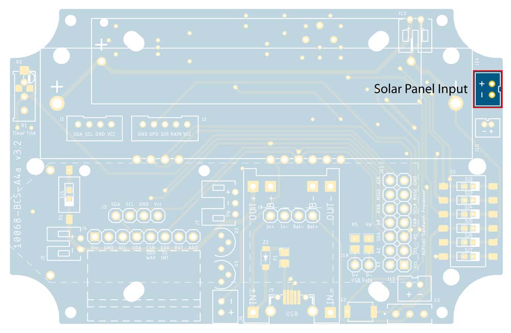 |
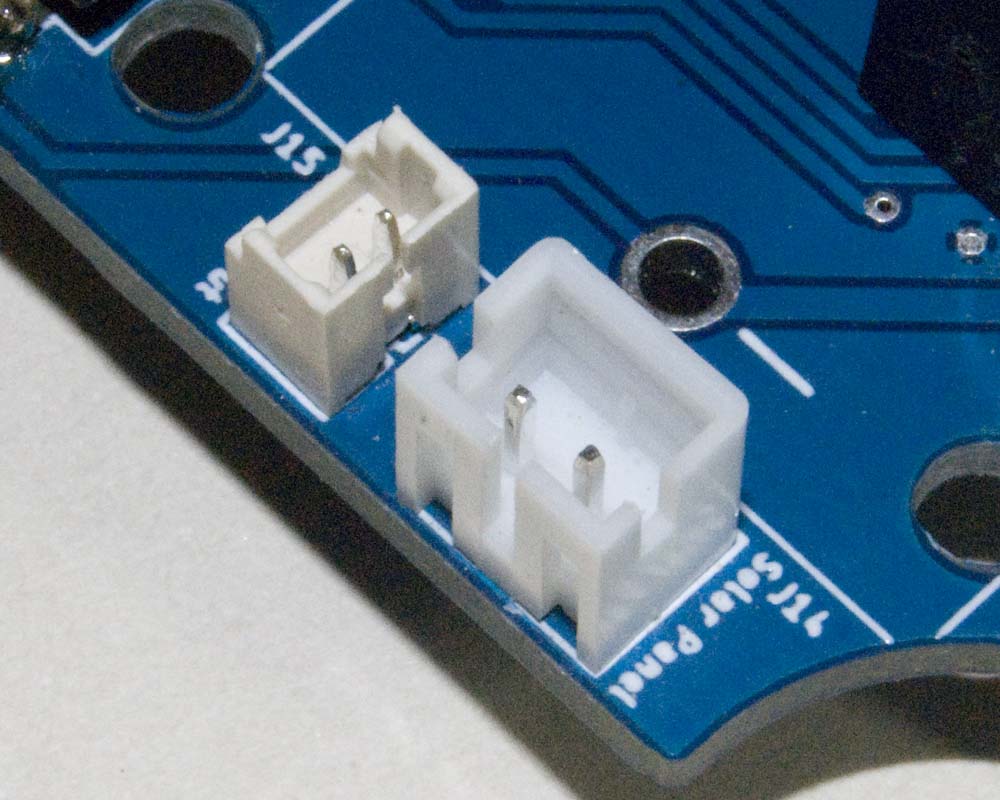 |
Solar Panel JST PH2.0 Connector
Solar panel connectivity is provided through a 2P JST PH2.0 connector (J14) configured in conjunction with a 1N5819 Schottky diode (Z2) for reverse current protection of the solar panel.
I realise that there is some commentary that suggests that one should not charge a battery while it's in use. I'm not sure what the problem is here, whether this is a 'purist' thing or if the battery can be damaged somehow. I've certainly not noticed any problems, as such, with my present configuration. The reality is that the node is only active for a second or so every minute (during testing, and ultimately a second or so every 10-15 minutes when in operation) so, for the most part, the node is not drawing any significant current while the battery is charging.
One thing I have noticed though is that the solar panel will never fully recharge a depleted battery. This may have something to do with one particular configuration that draws more power than others because, for the most part, as long as the sun shines for a few hours every couple of days (not a real problem here in Australia), my batteries stay fully charged.
Power Output
 |
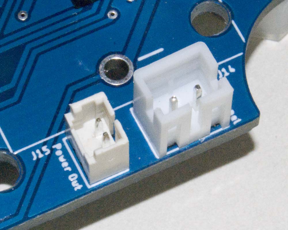 |
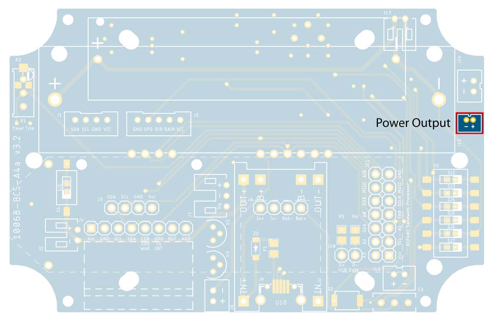
Power Output JST GH1.25 Connector
Processor boards that have inbuilt power management systems that require independent power input can be supported through a JST GH1.25 connector (J15).
The Heltec CubeCell, for example, is entirely self contained from a power perspective and requires only a simple battery connection—it does not need any external charging or battery protection circuitry. It also has its own solar panel input and supporting battery charge management hardware (the CubeCell doesn't actually need any of the features of the present PCBs other than the sensor interface(s)—see below).
Note that the orientation of the positive and negative pins in the Power Output connector is the opposite to that of other power connectors. The wiring of the Power Output connector is configured to be consistent with Heltec development boards, which have a matching JST GH1.25 connector for power input. Other (JST PH2.0) power connectors, like the LiPo and solar panel connectors, are configured to be consistent with the wiring on LiPo batteries.
MT3608 Boost Converter
| Top (Water Level JST) | Bottom (Boost Converter/INA219) |
|---|---|
 |
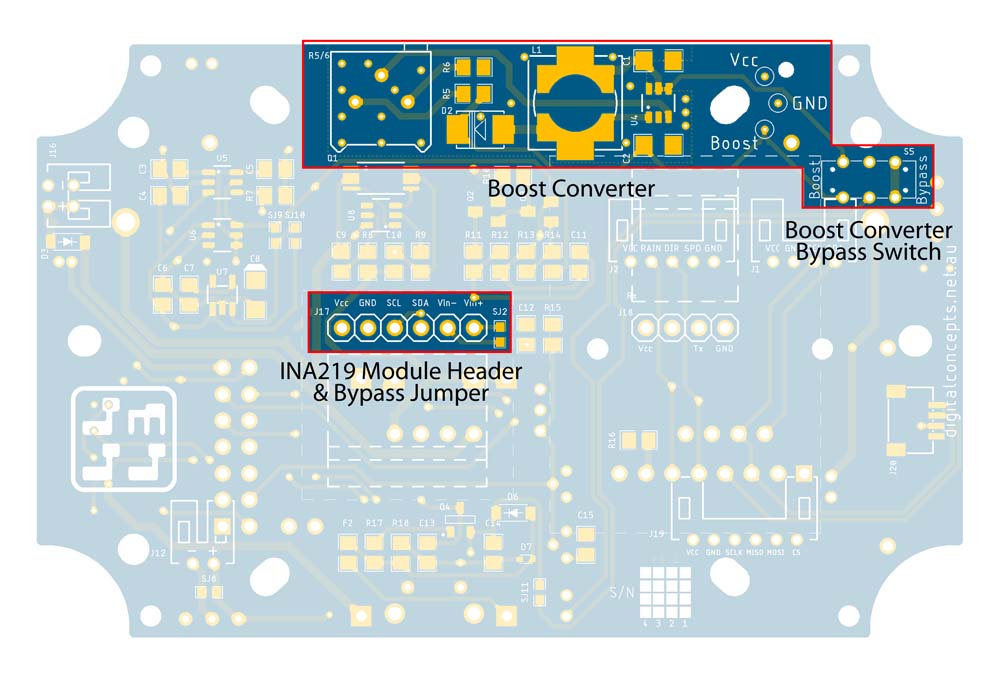 |
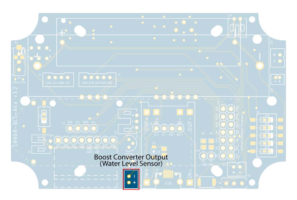
Boost Converter Circuit Elements [v3.2]
Boost Converter [v3.0 – see above for current v3.2 layout]
The MT3608 (U4) boost converter circuit can be configured to provide a 3.3V-28V power source or bypassed, or simply not configured, as required.
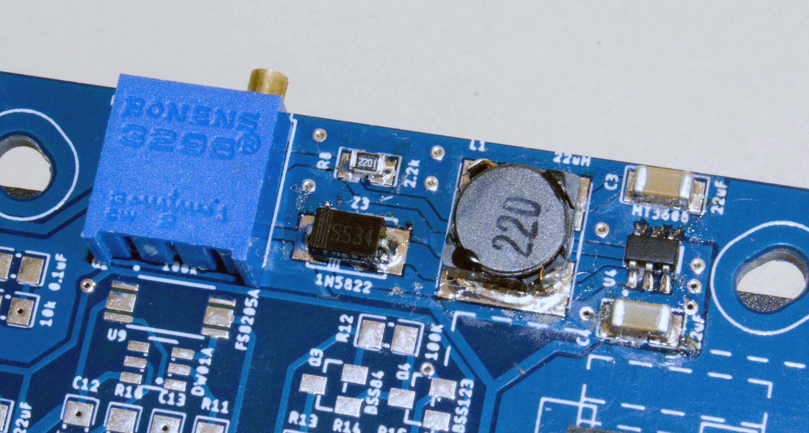
The boost converter circuit itself comprises the MT3608 IC (U4), 22µH inductor (L1), 1N5822 Schottky diode (D2), the 2k2Ω (R5) and 82K (R6) resistors, the 10kΩ trimpot (R5/6), and the two 22µF capacitors (C1 & C2).
This circuit is based on that used in a commonly available MT3608 boost converter module and is provided to support a 24V HDL300 (or similar) water level sensor. I actually did the original breadboard work with the module, then created an 'on-board' circuit to save space.
I don't really know how much of the present layout is essential but my original efforts, where I did not pay any attention to layout, were spectacular failures. In working through why things went wrong, I resorted to the MT3608 datasheet, which provides guidance on circuit layout. As noted, the early layouts, where I just arranged all of the components neatly, were quite unstable—I could never reliably get the output voltage anywhere near 24V. When I placed the inductor and capacitors close to the MT3608 IC, and included the ground plane, things worked much more reliably.
I have also subsequently modified the boost converter circuit slightly by adding an extra resistor to the output circuit to provide more sensitivity in setting voltage levels. The original configuration, as per the commercially available module, used a 100kΩ trimpot, but only about 20% of its range was useful. By inserting the additional resistor and using a 10kΩ trimpot, most of the range of the trimpot can be used, allowing the output voltage to be set more precisely (for what that might be worth).
Boost Converter Output Voltage
From the MT3608 datasheet, the output voltage is determined by the values of the resistors in the output side of the boost converter circuit, according to the following equation:
| Vout | = | Vref × | ( | 1 + | R1 R2 | ) |
where the internal reference voltage Vref is typically 0.6V and the values of R1 and R2 are determined, in our case, by the values of resistors R5 and R6 and the setting of the trimpot R5/6.
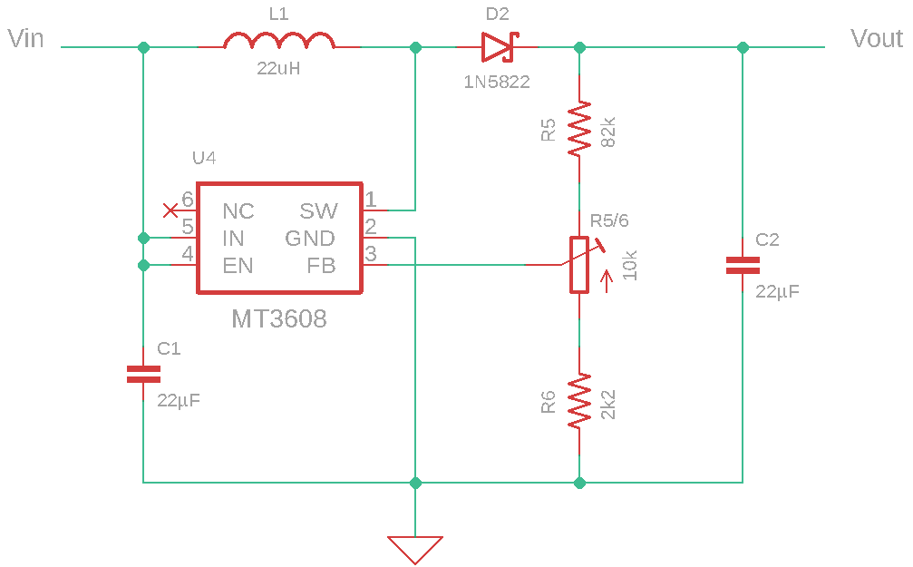
Boost Converter Circuit
The following table lists the theoretical output voltage across the range of the 10kΩ trimpot.
Theoretical Vout Values
| R1 | R2 | Vout (V) | ||
|---|---|---|---|---|
| R5 (kΩ) | Trimpot (kΩ) | R6 (kΩ) | ||
| 82 | 10 | 0 | 2.2 | 28.4 |
| 9 | 1 | 19.5 | ||
| 8 | 2 | 14.9 | ||
| 7 | 3 | 12.0 | ||
| 6 | 4 | 10.1 | ||
| 5 | 5 | 8.7 | ||
| 4 | 6 | 7.6 | ||
| 3 | 7 | 6.8 | ||
| 2 | 8 | 6.1 | ||
| 1 | 9 | 5.6 | ||
| 0 | 10 | 5.1 | ||
I've also included 'tap points' close to the boost converter circuit to facilitate the setting of the boost converter output voltage—assemble the circuit then use a multimeter to measure the Boost–GND voltage while adjusting 10kΩ trimpot (R5/6).
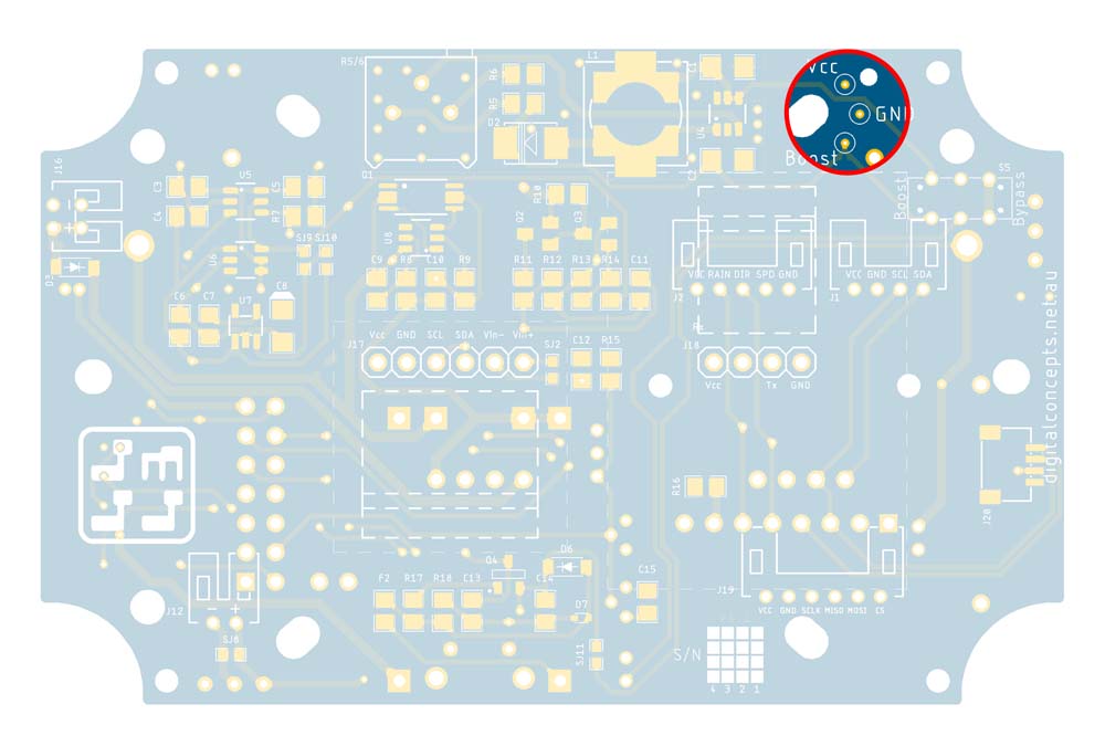 |
Voltage Measurement Points
The boost converter output, or simply the battery output if the boost converter is bypassed, is connected directly to the 2P JST2.0 [Water Level] connector and then to the INA219 module that is plugged into the 6P header on the base of the board. The INA219 module is thus used to measure the current in this circuit.
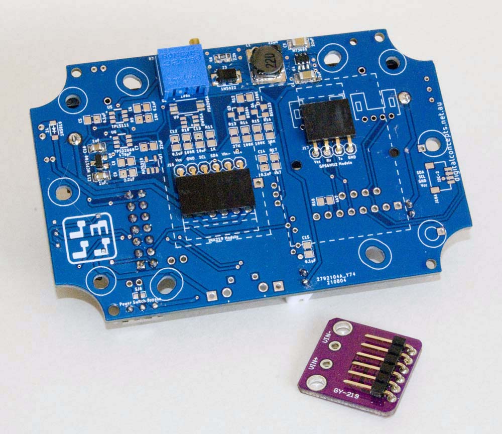 |
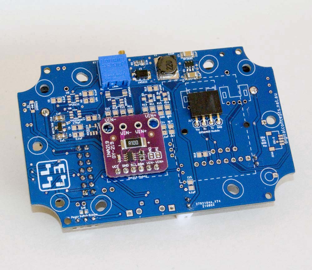 |
INA219 Module
Low Power Switch/Timer
The TPL5111 timer and TPS22860 switch or MIC5219 regulator can be configured in combination to provide a low power option that can be used to cut power to the processor and sensors between sensor readings and packet transmissions.
TPL5111 Timer
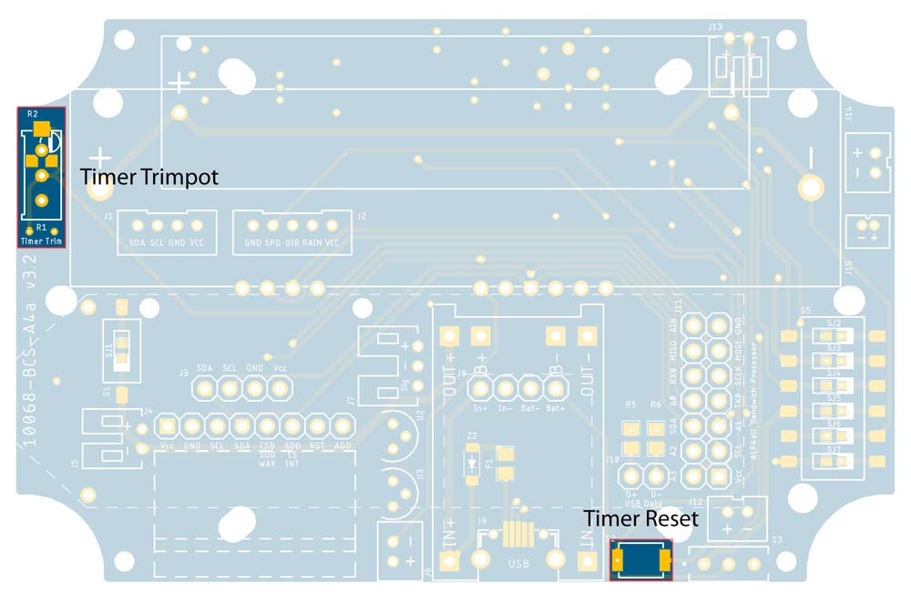
| Top (R1/R2 Trimpot & Reset Button) | Bottom (IC, C6 & R9) |
|---|---|
 |
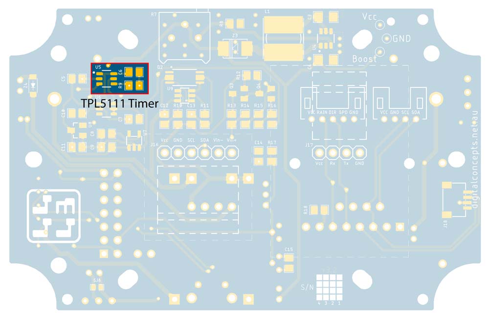 |
TPL5111 Circuit Components
The TPL5111 Timer (U5) can be configured, with or without the TPS22860 Switch or MIC5219 regulator or all of these components omitted altogether, to suit the application at hand.
If configured, capacitor C6 (100nF) and resistors R1 (or R2) (variable Ω) and R9 (10kΩ) are also required. R1/R2 is a variable resistor that allows the timer interval to be adjusted.
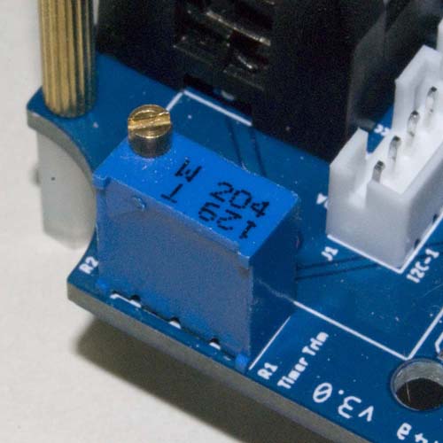
The current PCB layout includes two alternate variable resistor configurations—a physically larger, more finely adjustable BOURNS (or BONENS clone version) component (R1), or a smaller SMD component (R2) with 'less refined' tuning.
| BOURNS/BONENS | SMD |
|---|---|
 |
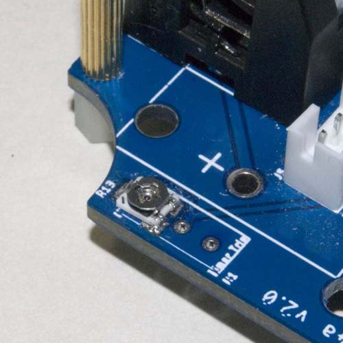 |
Timer Trimpot Alternatives
The resistance of the trimpot can be chosen to provide the level of sensitivity or duration of time required. The forumla used to determine the relationship between the value of R1 and the elapsed time is provided in the TPL5111 Datasheet, but some typical resistor values and associated timings are provided in the following table.
Time vs Resistance
| Delay | Resistance (kΩ) |
|---|---|
| 2s | 6.8 |
| 3s | 7.6 |
| 20s | 14.4 |
| 30s | 16.8 |
| 1m | 22.0 |
| 2m | 29.4 |
| 5m | 42.9 |
| 10m | 57.4 |
| 20m | 77.6 |
| 30m | 92.4 |
| 1h | 124.9 |
| 2h | 170.0 |
The BOURNS/BONENS trimpots provide about 26 full [360°] turns of adjustment, from zero to maximum resistance—that's a little less than 4% of the rated resistance per 360° rotation of the trimmer knob. They usually come preset at around the centre of their range. For a 200kΩ trimpot, the resistances are roughly as listed in the following table, starting with the trimpot turned fully anticlockwise then for each 360° clockwise rotation on the trimmer knob.
Trimmer Setting vs Resistance
| Turns Clockwise | Resistance (kΩ) |
|---|---|
| 0 | 0 |
| 1 | 7.3 |
| 2 | 15.8 |
| 3 | 24.0 |
| 4 | 31.5 |
| 5 | 39.3 |
| 6 | 46.6 |
| 7 | 55.3 |
| 8 | 62.8 |
| 9 | 71.7 |
| 10 | 79.7 |
| 11 | 87.9 |
| 12 | 92.1 |
| 13 | 99.8 |
| Turns Clockwise | Resistance (kΩ) |
|---|---|
| 14 | 109.3 |
| 15 | 116.3 |
| 16 | 124.1 |
| 17 | 131.9 |
| 18 | 139.9 |
| 19 | 147.2 |
| 20 | 154.5 |
| 21 | 162.5 |
| 22 | 169.7 |
| 23 | 177.5 |
| 24 | 184.8 |
| 25 | 191.6 |
| 26 | 203.1 |
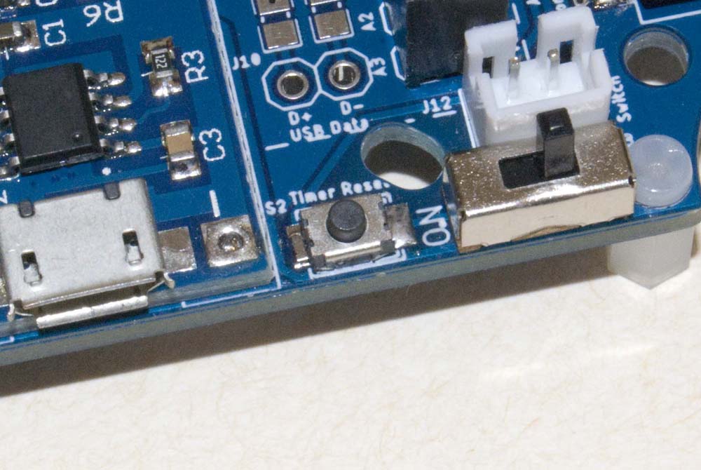
An optional reset button can also be configured to manually trigger and reset the timer.
Timer Reset Button
As noted earlier, the TPL5111 timer can be configured without the TPS22860 switch or MIC5219 regulator, but there is no particular benefit in any of the present applications in doing this.
TPS22860 Switch
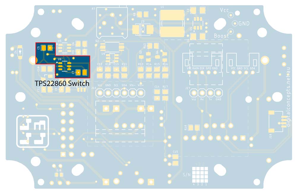 |
TPS22860 Circuit Components
The TPS22860 (U6) Switch circuit, which includes capacitors C5 (100nF) & C7 (22µF), can be configured or bypassed as desired. By default, the TPS22860 switch is 'in circuit', but two other circuits generally need to be activated in order to control the operation of the Switch and Timer.
The DONE circuit is used, by the node's processor, to trigger the Timer, which in turn turns off the Switch. The WAKE circuit is used, if required, to reactivate the processor when the Switch is again turned on.
DIP Switch Settings – Switch Circuit Configured
The Switch DIP switch, if configured, or bridging of the solder jumper, if not, can be used to bypass the TPS22860 switch circuit.
DIP Switch Setting – Switch Circuit Bypassed
Having now assembled several node configurations, it is clear that the MIC5219 regulator serves the same function as the TPS22860 switch circuit, while also regulating the voltage.
According to their respective datasheets, however, the quiescent current drawn by the TPS22860 is ~10nA, while that of the MIC5219 is 50–100nA. On the other hand, the TPS22860 load switch costs ~A$1.20 while the MIC5219 regulator costs just A$0.10, maybe not so much a consideration for a one-off project but perhaps more important if producing nodes in volume.
Either way, only one of these options is required in any individual circuit to power it down when inactive.
Voltage Regulator
Either of two [3.3V] regulator options can be configured if required—no regulator is required, for example, if using a LiFePO4 battery. The early versions of the BCS boards only used the MCP1700 regulator. The MIC5219 option was added with the timer elements because it could be switched off when not in use. Both options remain because the MCP1700 is a simple 'set and forget' alternative when that is all that is required.
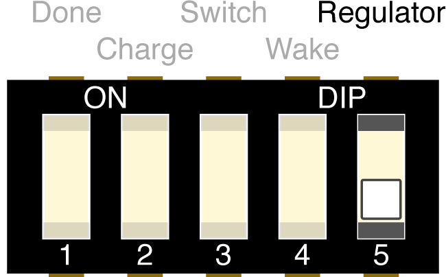
The voltage regulator circuit can be configured or bypassed as desired, independently of the timer/switch circuit. By default, the regulator circuit is 'in circuit'.
DIP Switch Setting – Regulator Configured
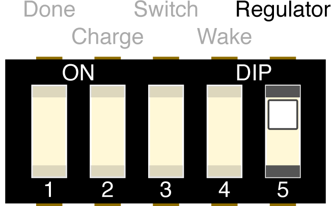
If no regulator is configured, the regulator circuit needs to be bypassed. The Regulator DIP switch (Main Bank DIP switch 5 in the ON position), if configured, or bridging of the solder jumper SJ6, if not, can be used to bypass the regulator circuit.
DIP Switch Setting – Regulator Circuit Bypassed
MIC5219 Voltage Regulator
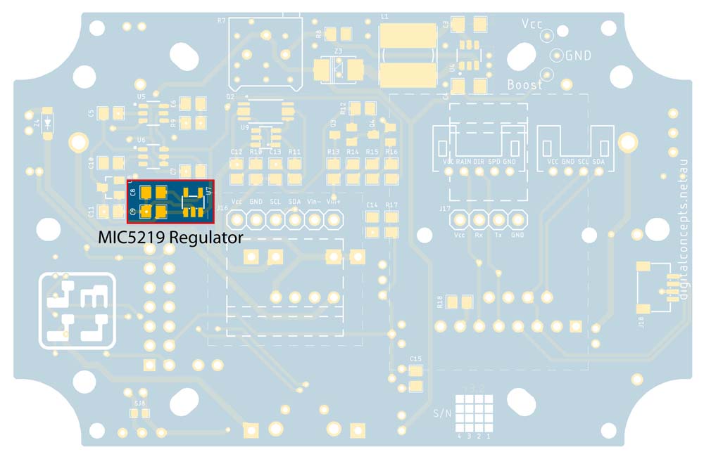 |
MIC5219 Circuit Components
The MIC5219 regulator (U7) is a low dropout linear voltage regulator that can be enabled or shut down by an external trigger signal. This regulator circuit, which includes capacitors C8 (470pF) and C9 (2.2µF), is thus activated by the timer circuit to minimise quiescent current leakage.
MCP1700 Voltage Regulator
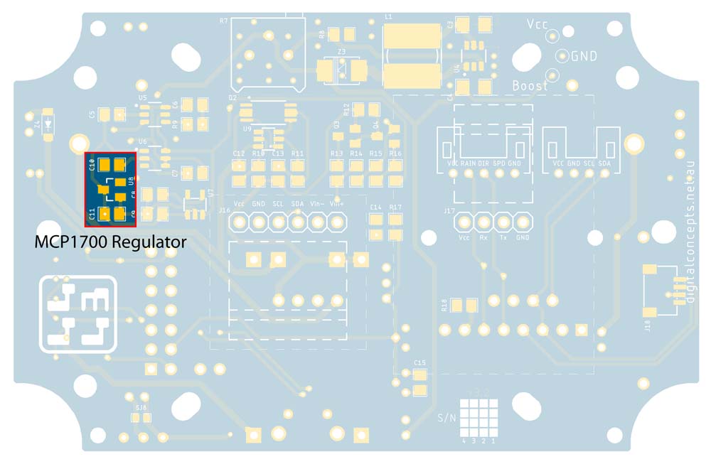 |
MCP1700 Circuit Components
The MCP1700 [3.3V] regulator (U8) is a low quiescent current (1.6 µA) low dropout voltage regulator that can be used as an alternative to the MIC5219. This regulator circuit includes capacitors C10 (1µF) and C11 (1µF).
Sensor Configuration
ALF4all Sensor Interface
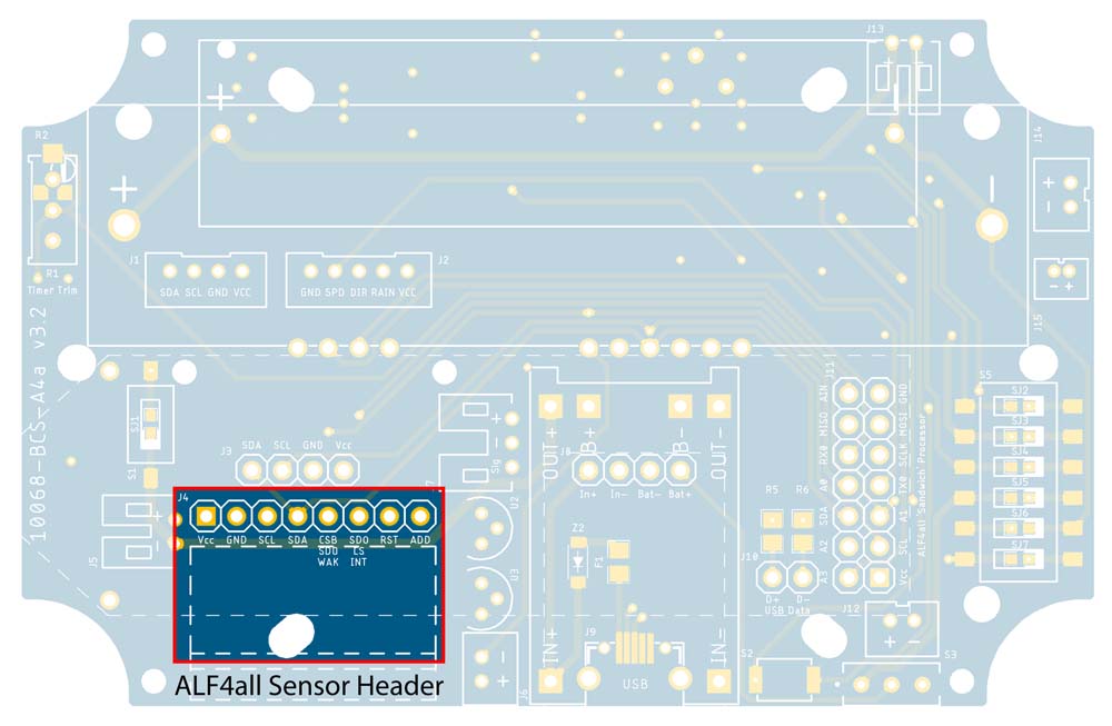
The main sensor interface is provided through an 8-pin female header configured in accordance with the Wijnand Nijs ALF4all sensor interface. It supports a range of sensors, using several different interace configurations, including any that use an I2C interface (left-most 4 pins of the header).
ALF4all Sensor Interface Configuration
 |
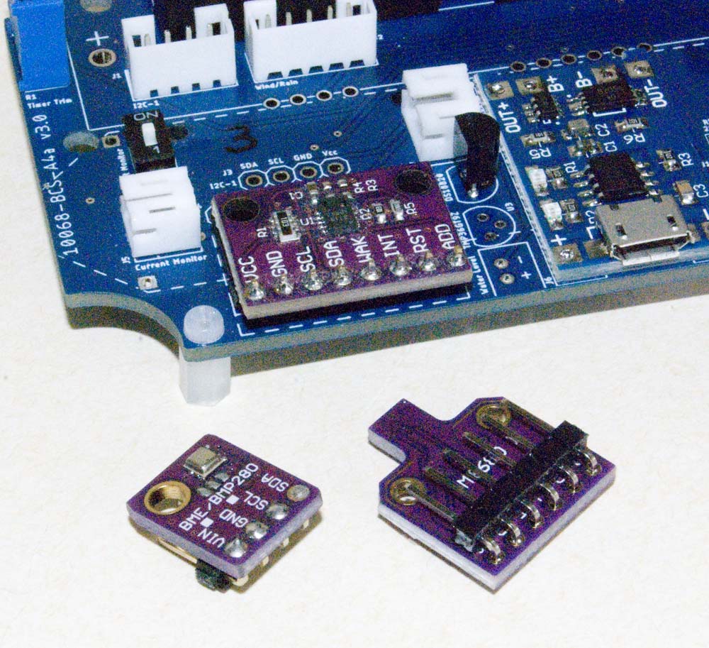 |
ALF4all Sensor Interface
One of the features of the BCS-A4a boards is the right-angle headers that are used throughout for sensor module configuration. By laying the headers down in this way, it was possible to support the ability to dynamically configure different sensor modules using pretty much the same amount of vertical real estate as a fixed module. The general intention is that sensor modules are configured with a mating right-angle male header. This configuration also supports for the convenient use of adaptor boards for different pin configurations (see I2C Interface and Air Pressure Sensor). There is, nonetheless, enough room to attach most sensor modules, particularly any with bulky components on both sides, in a vertical position (with straight male headers).
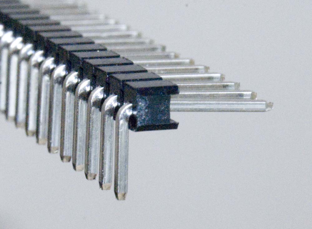
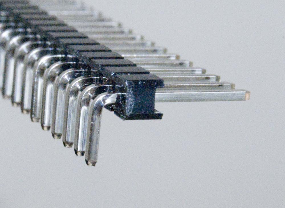
When purchasing right angle headers, note that there are three different configurations of male right angle header as illustrated below.
| This is the one I generally use | ||
|---|---|---|
 |
 |
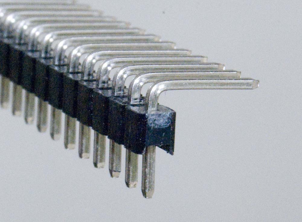 |
Male Right Angle Header Configurations
I2C Interfaces
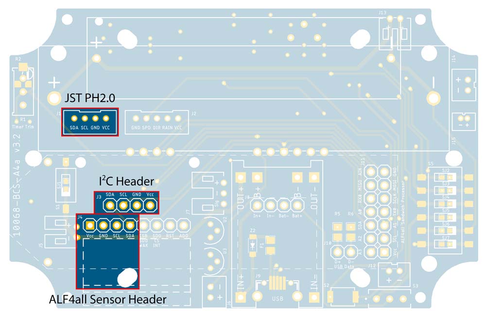
| Top | Bottom |
|---|---|
 |
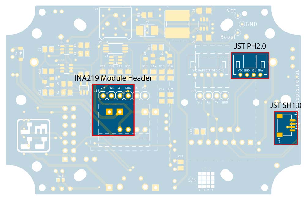 |
I2C Connection Points
Several I2C connection points are provided on the BCS-A4a board. They include:
- The left-most 4 pins of the A4a Sensor header (see above)
- A dedicated I2C header (located adjacent to the A4a Sensor header—can also be configured on the reverse side of the board of the NEO-6M GPS module is not configured)
- The left-most 4 pins of the INA219 module header
- A JST PH2.0 socket (not available on board obverse if 18650 battery holder configured, or board reverse if NEO-6M GPS header configured)
- A JST SH1.0 socket on the base of the board
| Interface | |
|---|---|
| A4a Sensor Header | 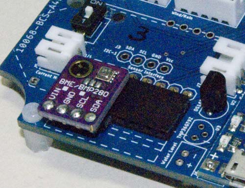 |
| I2C Header | 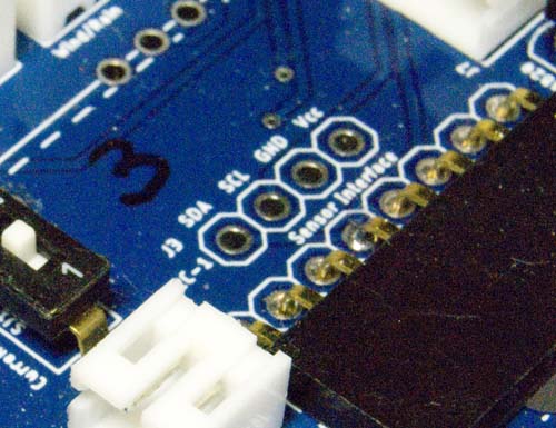 |
| INA219 Header | 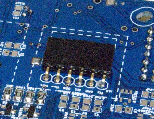 |
| JST PH2.0 Socket | 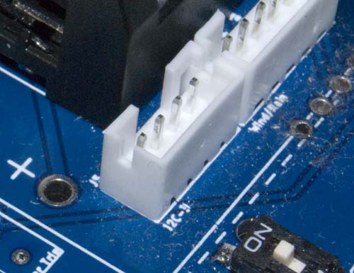 |
| JST SH1.0 Socket | 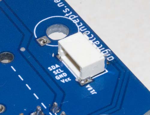 |
I2C Sensor Interfaces
The JST SH1.0 socket was included simply to see how easy it was to both [hand] solder the SMD component and to use the associated cables. The locking mechanism on the JST PH2.0 sockets can make the removal of cables a bit fiddly at times, especially when the socket is located in a confined space. The smaller SH1.0 sockets don't have any such locking mechanism and turn out to be easier to use in that regard. Their size and surface mount nature also means that they use less board real estate, so I might make more use of them in the future. The down side is that cables are more difficult to make by hand, but this is really only a nuisance during prototyping. Once a cable configuration is set, it's easy enough to buy the necessary items preconfigured.
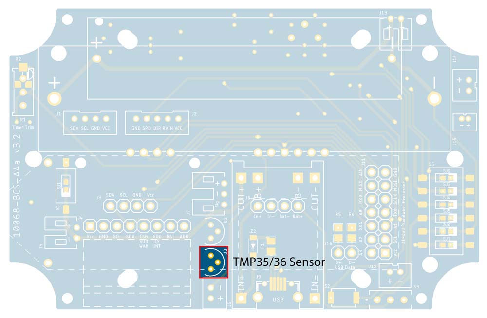
TMP35G and TMP36GZ Temperature Sensors
| Top (TMP35/36) | Bottom (C15) |
|---|---|
 |
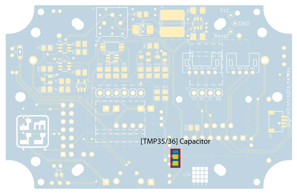 |
TMP35/36 Components
TMP36GZ Temperature Sensor
The TMP35 or TMP36 analog temperature sensors are soldered directly, in the space allocated, to the PCB. Capacitor C15 (0.1µF) should also be configured. Note that only one of the temperature sensor options (TMP35G/TMP36G or DS18B20) can be configured on a PCB because they share the same processor GPIO pin.
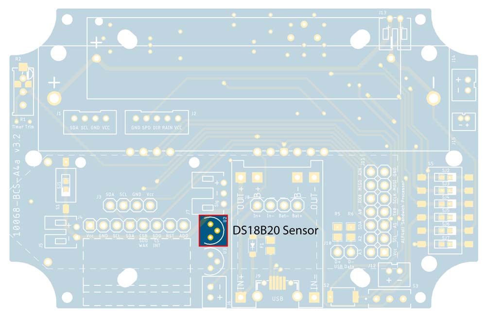
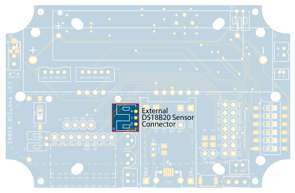
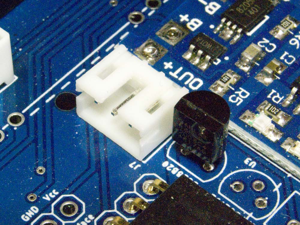
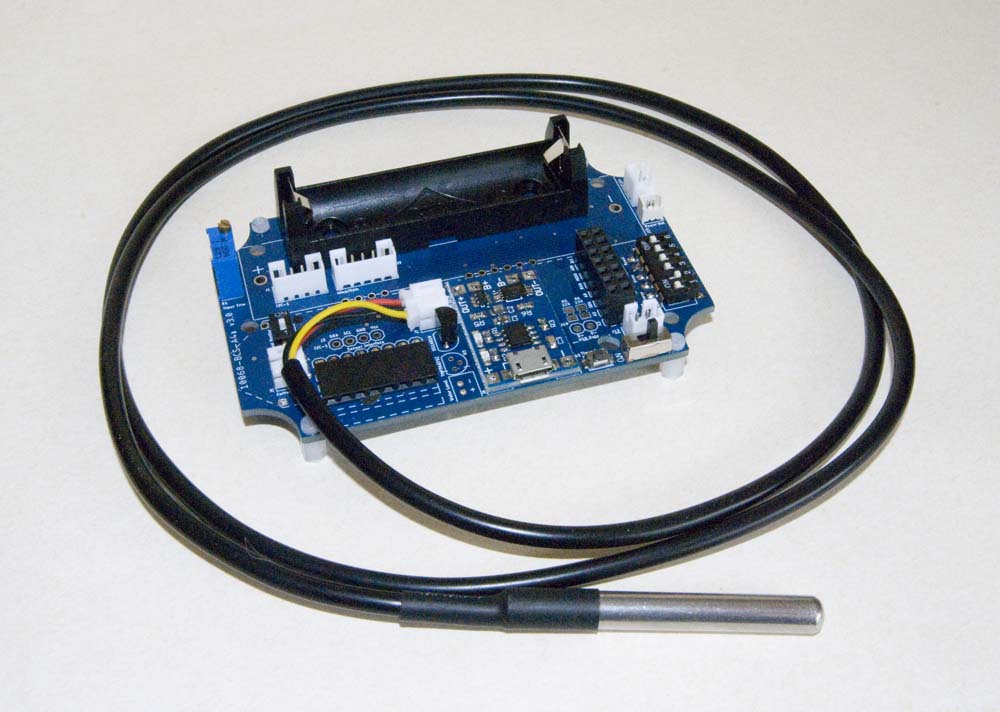
DS18B20 Temperature Sensor
| Top (DS18B20) | Top (External DS18B20 JST Connector) |
|---|---|
 |
 |
| Bottom (C14 & R17) |
|---|
 |
DS18B20 Components
| Internal | External |
|---|---|
 |
 |
DS18B20 Sensors
There are two varieties of this digital temperature sensor, one (the 'internal' version) that can be soldered directly to the PCB, in the space allocated, and the other (the 'external' version) that can be configured to plug into a 3-position JST PH2.0 connector. Both of these options require the configuration of capacitor C14 (0.1µF) and resistor R17 (4k7Ω for on-board sensors or short cables, or 2k2Ω for longer [2-3m or more] cables), in addition to the sensor and/or connector.
Note again that only one of the temperature sensor options—[analog] TMP35G/TMP36G or [digital] DS18B20—can be configured on any individual PCB, although multiple DS18B20 sensors can be configured as they are all individually identified on the [digital] onewWire bus to which they are connected.
Wind/Rain Sensors
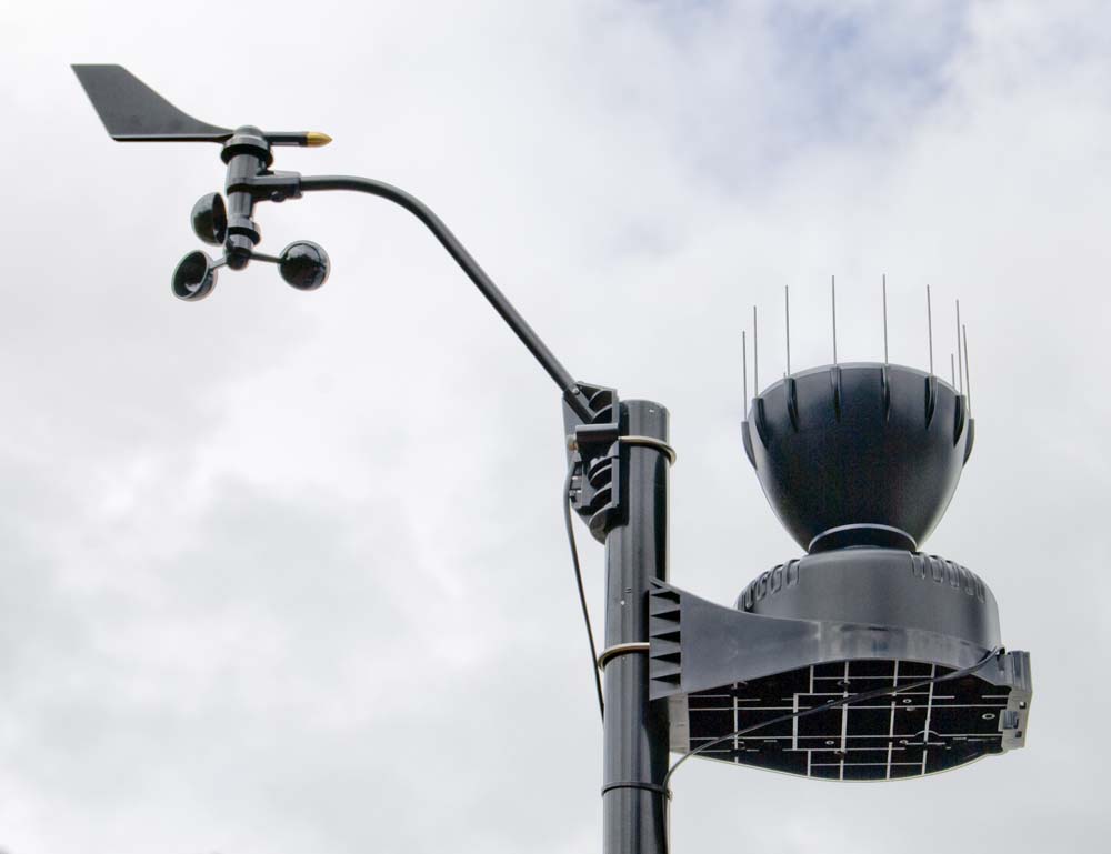
Davis Instruments Anemometer and Rain Collector
| Top | Bottom |
|---|---|
 |
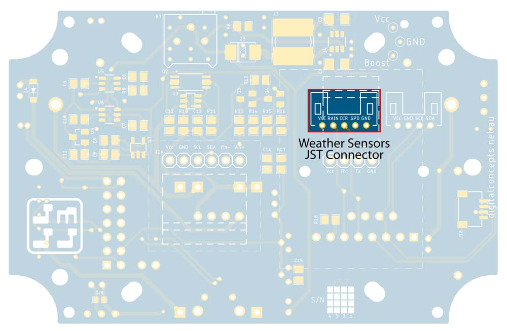 |
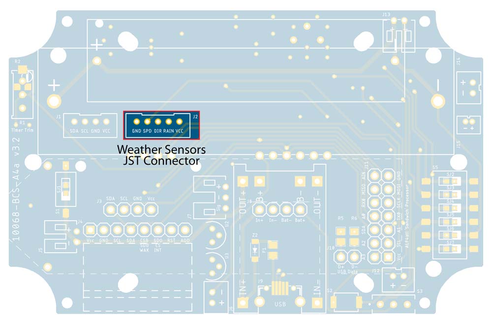
Weather Sensor JST Connectors
A separate 5P JST PH2.0 connector is provided for connection to the auxiliary 10068-WS PCB or other interface for wind and rain sensors. The connector can be configured on the top or the bottom of the board, as required. Note, however, that the connector on the bottom of the board is in the same general location as the NEO-6M GPS header, so only the top location can be used if the GPS header is also configured.
For my own application, I have used sensors from Davis Instruments, the 6410 anemometer and the 6466M rain collector (illustrated above).
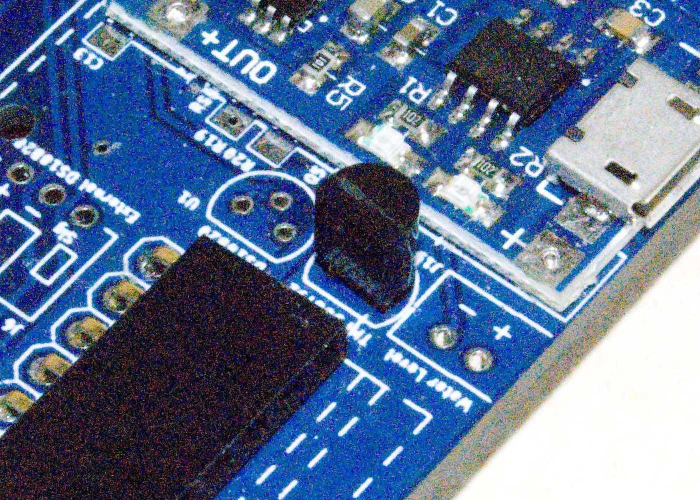
HDL300 [Water Level] Pressure Sensor
 |
Water Level Sensor JST Connector
HDL300 [Water Level] Pressure Sensor
I'm not sure if this is the most efficient way of doing this, but the 24V/4-20mA water pressure sensor requires both the boost converter to provide the required 24V power and an INA219 voltage/current sensor module with I2C interface to measure the current in the circuit. As such, this circuit can be used in a variety of ways. The I2C interface (the left-most four pins of the header) is just another I2C interface on the board and can therefore be used for any I2C device. Similarly, the boost converter can be used to power any sensor that requires anything from the 3.3V input voltage to around 30V in its present configuration.
NEO-6M/7M/8M GPS Module
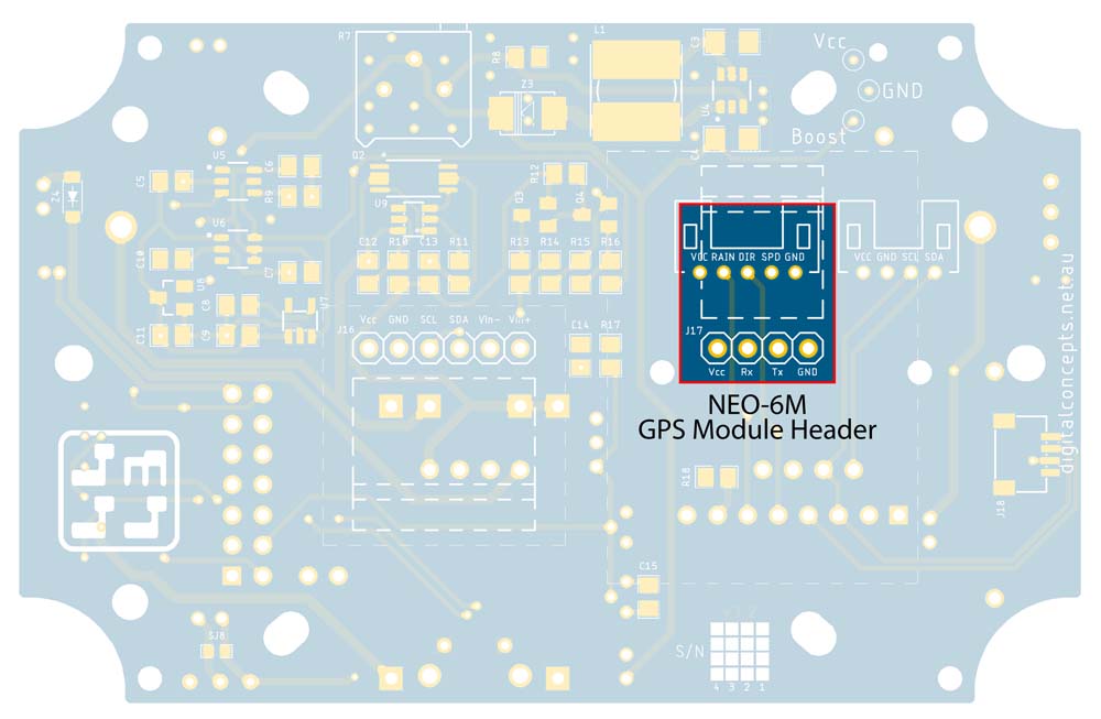 |
NEO-6M GPS Module Header
 |
 |
GPS Configuration
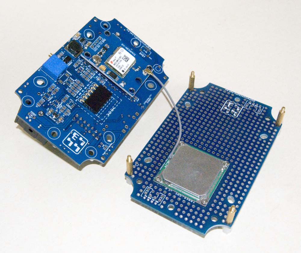
The BCS-A4a boards include support for a NEO-6M GPS module (which I believe is pin compatible with the later 7M and 8M models, but I have not tested these). The module slots into the 4-pin header on the rear of the BCS-A4a board. As with most of the sensor headers, the board is designed to use a right-angle female header, with the GPS module fitted with a mating right-angle male header. This keeps the packaging compact by allowing the module to sit flat on the BCS-A4a board.
The GPS Tx and Rx connections are provided through the ALF4all Sandwich interface to the supporting processor module.
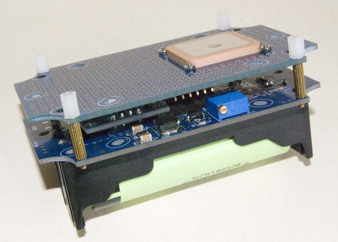
The 10068-GPSJ PCB is designed specifically to mount a 25mm GPS antenna and can be fixed onto the 10068-BCS-A4a base board with appropriate M2 stand-offs.


 Switch Setting.png)
 Bypass Switch Setting.png)

![HDL300 [Water Level] Pressure Sensor](../arduino/content/images/iot/assembly/10068-BCS-A4a/HDL300.jpg)