10068-BPS PCB
The BPS (Battery-Pi Zero-Solar) 'base' board is primarily designed to provide the Raspberry Pi Zero, including Raspberry Pi Zero W and Raspberry Pi Zero 2 W, processor boards with battery backup.
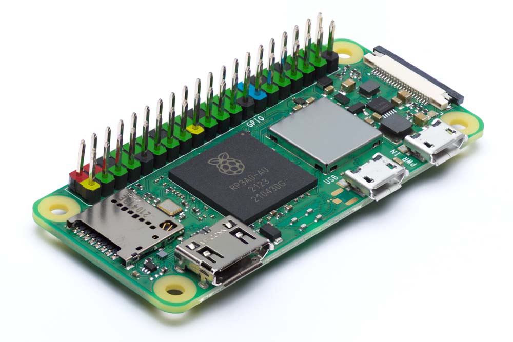
Board Layout
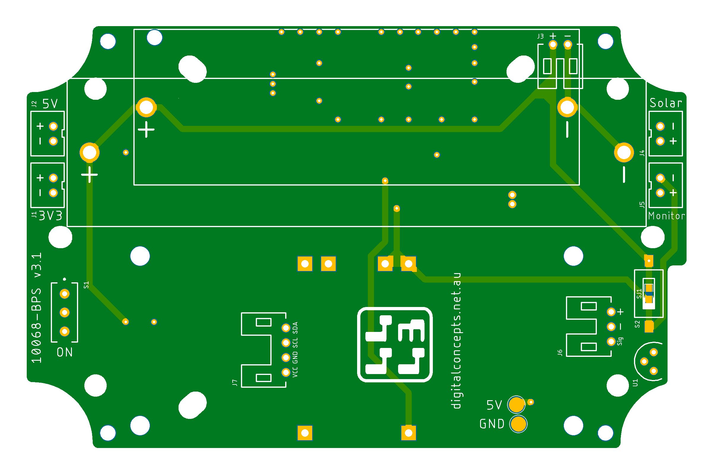
The various subsystems are identified in the board schematic and laid out as illustrated below:
| Top | Bottom |
|---|---|
 |
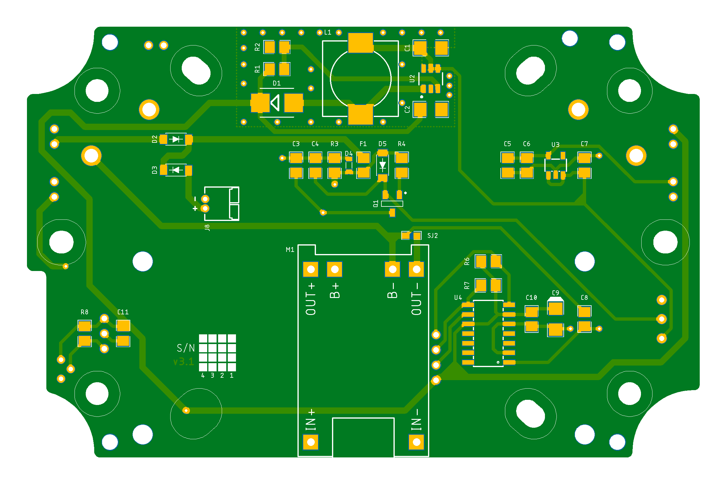 |
10068-BPS [v3.1] PCB
See here for CAD and CAM files.
This board is yet to be fully tested.
Configuration
The BPS board includes the following features:
- Mount points for Raspberry Pi Zero processor boards
- 5V 'pogo pin' connectors (for Raspberry Pi Zero [W])
- Support for 18500, 18650 and LiPo battery formats
- Power switch
- Regulator for 3.3V power
- MT3608 boost converter for 5V power
- 3.3V and 5V output JST PH2.0 connectors
- TP4056 battery charge management module
- USB and solar panel power input
- Automatic switching between external and battery power
- Battery voltage monitor (MCP3428 ADC)
- Current monitor tap point
- DS18B20 temperature sensor
Boost Converter
I originally had trouble building an on-board boost converter circuit (as distinct from using a preconfigured module) that worked 'properly'. I had tried several times already, on different boards, to build a boost converter circuit, but none of them was entirely satisfactory and I couldn't work out why. I thought I was just copying the circuit from a commercially available boost converter module. With the benefit of hindsight, I just wasn't copying precisely enough. When I copied the circuit faithfully, down to the individual component level, it worked as expected.
The MT3608 datasheet includes layout considerations that need to be observed, and I also found this TI Application Report useful.
The present boost converter design does now faithfully copy the circuitry of a common commercial module, with one exception—rather than a variable resistor for setting the boost converter output voltage, specific resistors must be soldered in place. I made this decision for two reasons. First, the only boosted voltage required on this board is 5V for the Raspberry Pi. The second reason is that I fried one of my Pi Zeroes when I incorrectly set the variable resistor on one of the boards—the variable resistor configuration, as provided on the commercial module, can be set to deliver an output voltage of up to 28V.
Other than this, the difference between this and previous iterations of the circuit is simply that the inductor, and the capacitors, are now the same physical size (CDRH104R and 1206 respectively) as those on the commercial module. Earlier iterations had used smaller components (CDRH6D28 and 0805) to save space, without realising the compromise that was being made—basically, the smaller components, while delivering the required voltage, seemed to be load-limited. They worked for for low current devices, like sensors that drew just tens of milliamps, but not for a Raspberry Pi, not even a Zero, that might be drawing several hundred milliamps during the boot cycle. The present configuration, which is essentially the same as that of the commercially available module, just with a fixed rather than variable output resistor configuration, is rated up to 2A.
Battery Charge Management
While I've never had a problem with using the TP4056 battery charging module to concurrently charge a battery and support a load current, I took the advice offered in this article, from TronicsBench.com, based on recommendations provided in Microchip Application Note AN1149, to use a P‑channel MOSFET 'switch' to separate the two functions.
It may be that my other projects have involved processors that spend most of their time in a low power or deep sleep mode, only drawing currents in the µA range, and that this is not enough to upset the battery charging cycle. Certainly, I have frequently observed the 'idle' LED glowing (blue in my case, but green on some modules), indicating that the charging cycle is complete, when the module has been connected to external power, either the USB connector or an active solar panel, while also charging the battery.
In the present case, however, it is anticipated that the processor being powered by this board would be supporting a gateway or server function and be continuously active —the battery would only be acting as a backup power source in case of mains power failure. This has the potential to create the problem described in the aforementioned article, where the load current is permanently in the mA range and may well inhibit the ability of the TP4056 to detect when the battery is fully charged.
I have read in one article that the circuitry of a boost converter obviates the need for separating the charging and load functions of the TP4056 module, but there was no explanation of why this might be and I have not seen this claim made anywhere else.
I also observed that the Heltec modules—WiFi LoRa 32, Wireless Stick [Lite] and CubeCell [Plus]—all use similar circuitry to that recommended, in their charging systems, with some additional components—the fuse, bidirectional diode and the resistor on the MOSFET gate—that provide improved overvoltage and ESD protection.
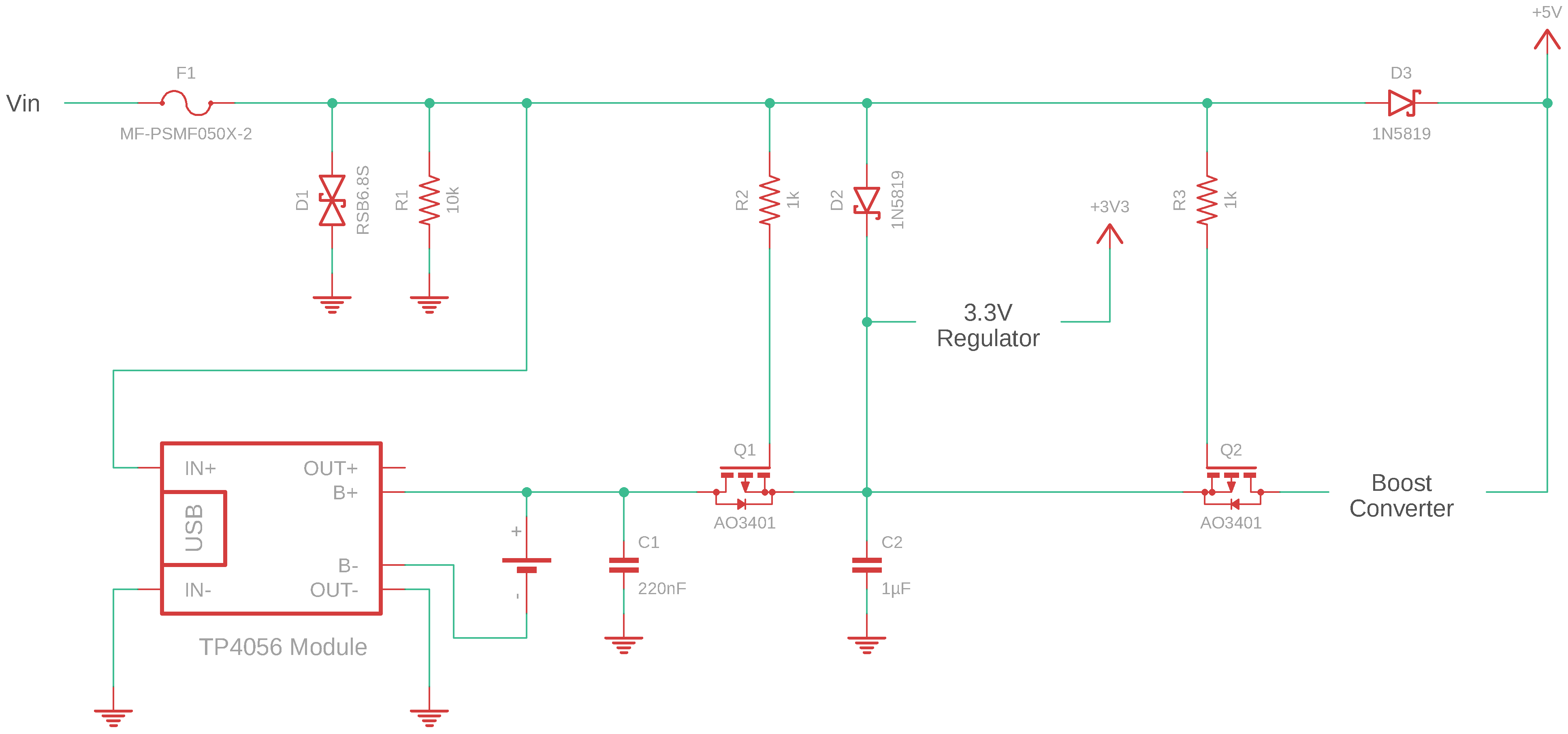
Power Circuit Source Switch
As can been seen in the above circuit, there were also some additional components, including the second MOSFET, that I initially thought would be needed in our case, because I thought we would only want the boost converter in the circuit when running from battery—the external [5V] supply, when connected, would feed directly into the 3.3V regulator and 5V rail.
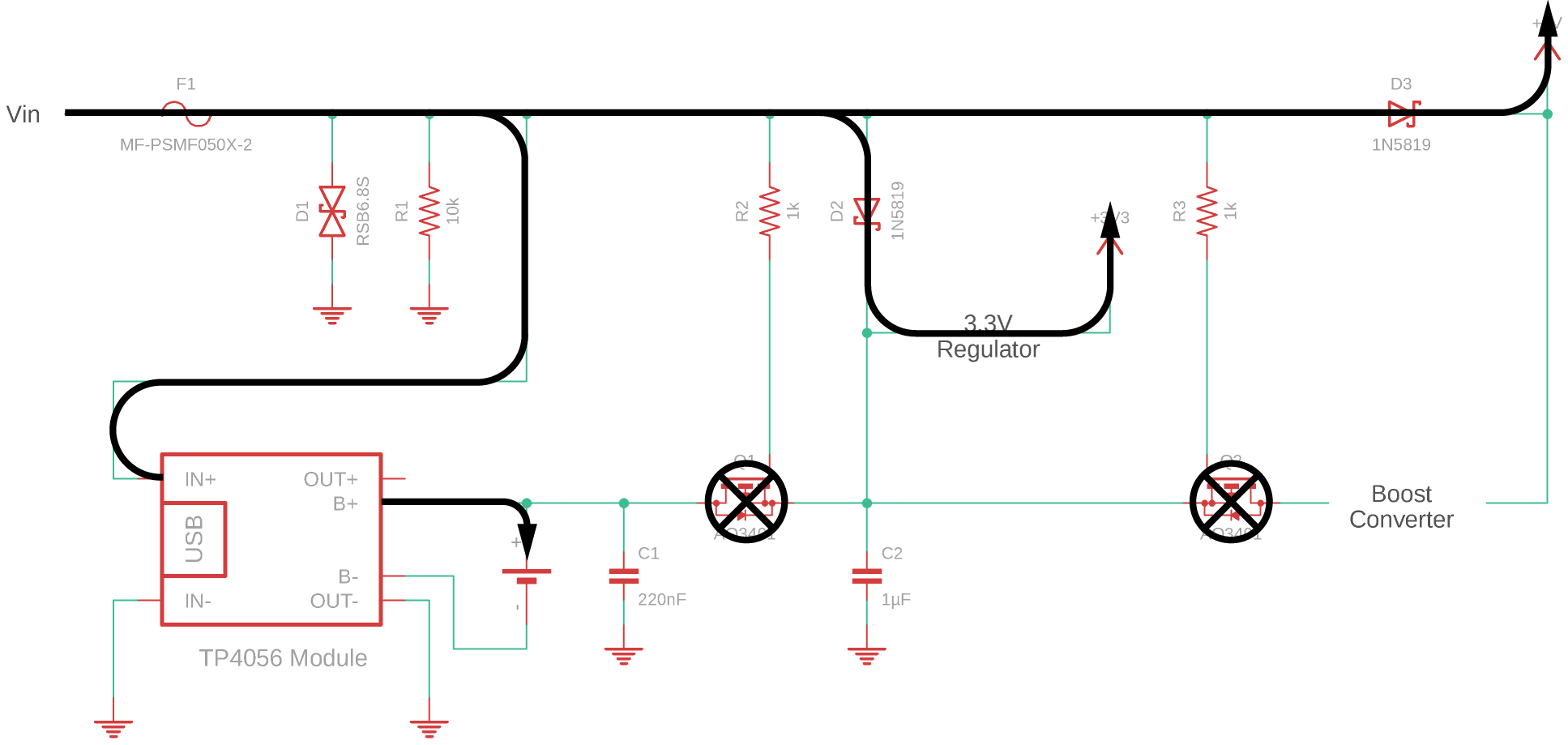
External Power
When there is no external power, and the circuit is powered by the [~3.7V] battery, the boost converter is switched into the circuit to provide the 5V supply.
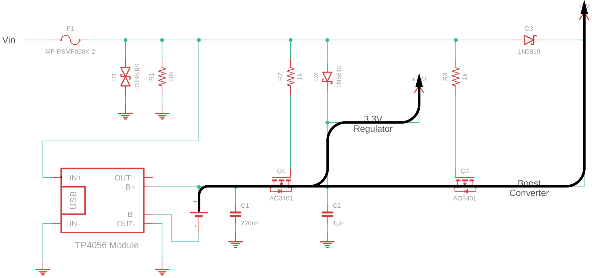
Battery Power
I was troubled for a time by the configuration of the first MOSFET (Q1) in this configuration. Even though this was also the configuration used on the Heltec dev-boards, it seemed to contradict my understanding of how a MOSFET worked. Generally, the power source is configured on the Source of a P-channel MOSFET, while the load is configured on the Drain, as is the case for the second MOSFET (Q2) in the above circuit.
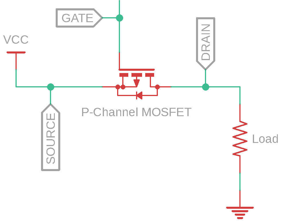
Conventional P-Channel MOSFET Switch Configuration
In the present case (Q1), the configuration seemed reversed—the apparent power source (battery) is connected to the Drain of the MOSFET, while the load appears to be connected to the Source.
At one point, I reversed the MOSFET configuration to match what I thought should be the correct configuration. While this initially appeared to work as intended, in that the MOSFET was switched OFF and ON when a voltage (Vin) was applied to the Gate, the fact that this voltage is invariably both greater than the battery voltage and is routed past the Drain of the MOSFET in this configuration, resulted in feedback through the parasitic diode in the MOSFET to the battery circuit—i.e. Vin, not the battery, should really be considered to be the power source in this case.
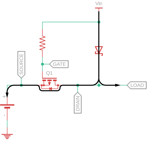
Behaviour of the Conventional P-Channel MOSFET Configuration
Using the arrangement of the MOSFET (Q1) in the original configuration above—connecting Vin to the Source of the MOSFET and the battery circuit to the Drain—avoids this feedback problem, which had the potential to disrupt the charging cycle, the very problem we are trying to avoid.
Even so, in practice things did not work entirely as expected. Although the external power source, usually a USB port, started out as a 5V source, by the time it had passed through the two zener diodes (in the circuit as implemented) it had fallen to 4.7V. While this seemed OK for the Pi Zero, the recommended range for a Raspberry Pi is 4.75 – 5.25V. Since the boost converter was there in any case, to boost the voltage supplied by the battery up to 5V, and since bypassing it involved additional circuitry, the logical thing to do was to forget about the additional bypass circuitry and simply feed all input through the boost converter. The circuit that has ultimately been implemented is as illustrated below.
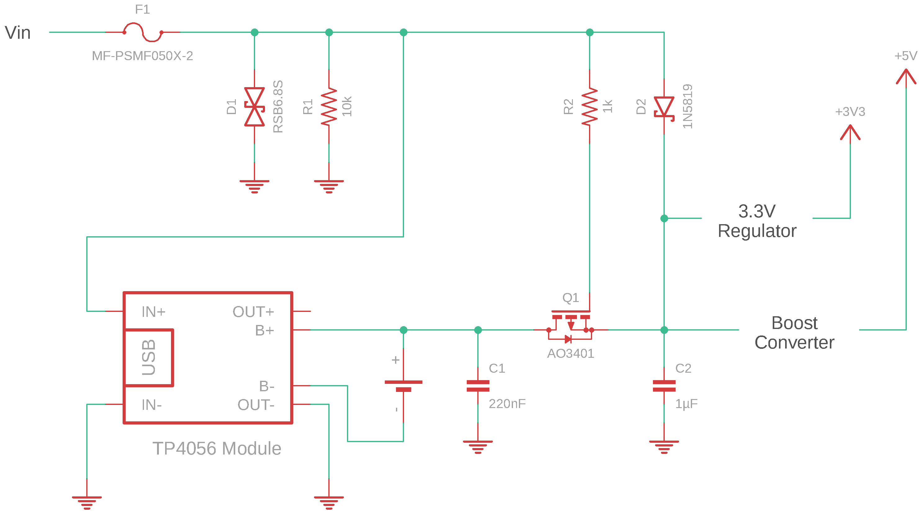
Power Circuit Source Switch as Implemented
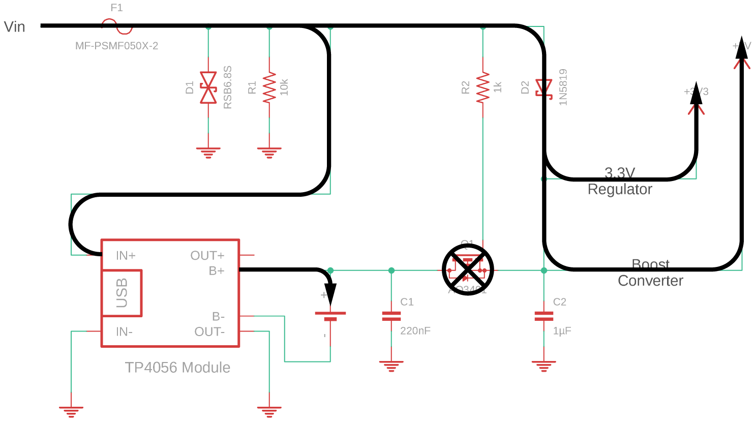
External Power
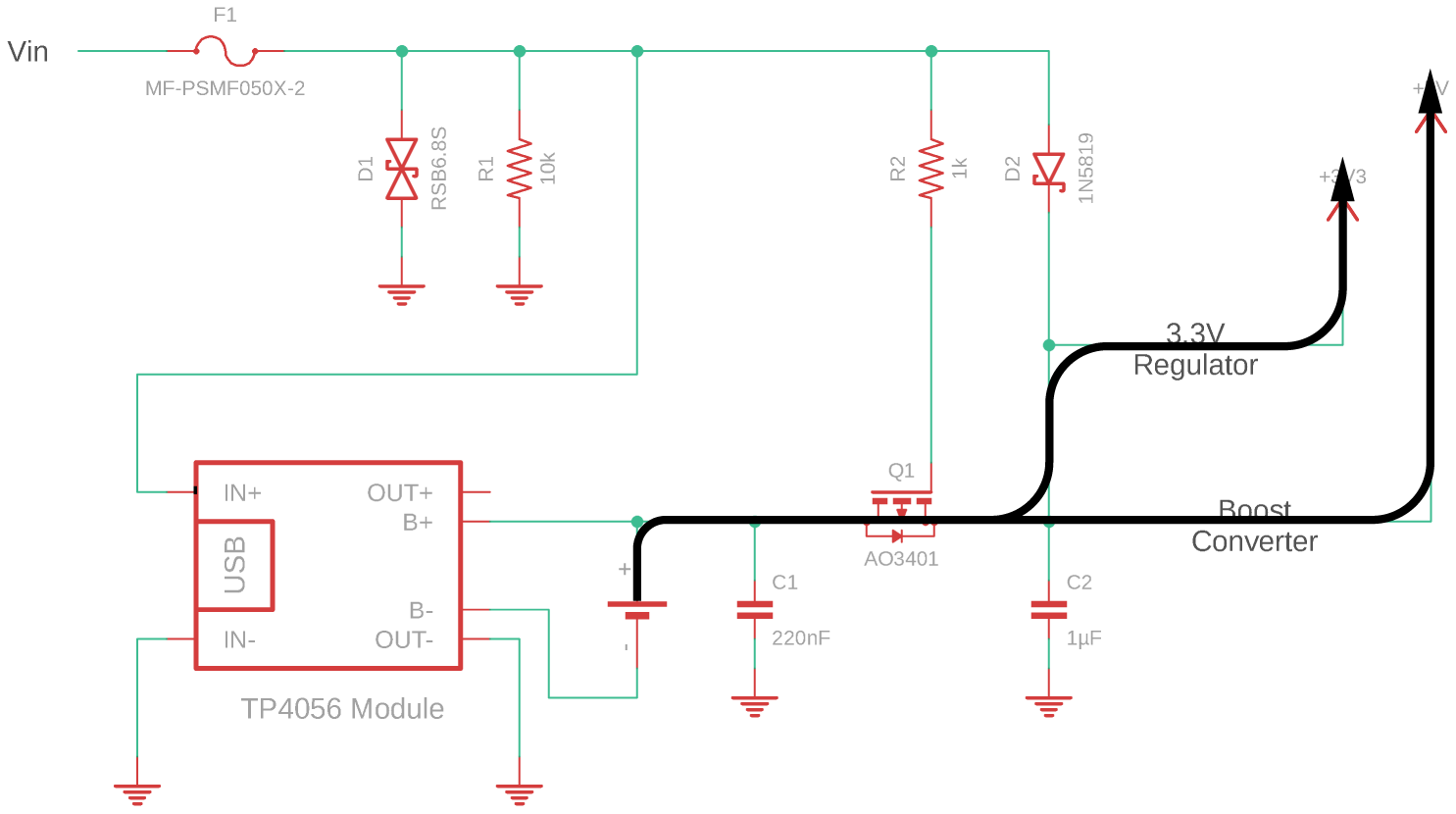
Battery Power
This latter circuit, on boards on which it has been configured, has been tested and works as intended.
Battery Voltage Monitor
Since Raspberry Pi MCUs only support digital I/O, analog measurements, like battery voltage, require the use of an external Analog-to-Digital Converter (ADC). An MCP3428, 4-channel, 16-bit ADC has been configured in the present case. Microchip do make a 2-channel version but, for some reason, it is more expensive than the 4-channel version and the real estate saving provided by the 2-channel IC (SOIC-8 vs SOIC-14) was not considered important.
Another feature of the Microchip device was the fact that it is connected to the Pi through an I2C interface and thus would not require the use of any additional GPIO pins.
Power Supply
OK, so it took me a few cycles around this problem to get to where I ended up. Initially, I had the 3.3V regulator providing input to the boost converter, which in turn provided input to a 5V regulator. I was troubled by the idea of a cycle that would regulate the voltage down to 3.3V, then boost it up to something like 6.5V to then have it regulated back to 5V. I spent some time reasoning through why a regulator might be needed on either the input or output of a boost converter and ultimately came to the conclusion that it wouldn't be, provided of course that the input voltage was within the specified range of the boost converter. While my education does not allow me to understand exactly why at this point, and I have not [yet] been otherwise able to confirm my suspicions, I have concluded that:
- All devices have their limitations and these are assumed to have been accommodated when making the following, further assumptions;
- A boost converter is a regulator in its own right—the formula provided to calculate the output voltage of a boost converter:
is not dependent on the input voltage. As such, a boost converter does not require a regulated source, nor does it require its output to be further regulated;VOUT = VREF × ⎛
⎜
⎝1 + R1
R2⎞
⎟
⎠ - Power provided through a USB socket is 5V and does not require any further voltage regulation to deliver 5V—either way, I couldn't see how to get any head room in a USB-powered circuit to enable it to be regulated 'back down' to 5V.
These conclusions then lead to the following design considerations for the proposed power supply board:
- Battery voltage, a nominal 3.7V for a Li-Ion battery, must be regulated to provide a 3.3V supply and boosted to provide a 5V supply. For the MT3608 boost converter IC, with VREF = 0.6V, using R1 = 75kΩ and R2 = 10kΩ will generate a 5.1V output, within the 5V ± 5% range recommended for the Raspberry Pi;
- 'USB' power, a nominal 5V supply from an 'external' USB port to a 5V pin on the Pi (not the USB port on the Pi), can be further regulated to provide 3.3V but could provide 5V directly. As noted above, however, the inclusion of protection diodes in this power circuit brings this supply voltage back to ~4.7V, so it was considered prudent to also feed this through the boost converter;
- Any over-voltage protection in the USB or direct power input circuits will need to be provided by a fuse or similar.
The 3.3V regulator and power output included on this board are entirely optional. They were included in case I had to use something that required a 3.3V supply. I am yet to identify any such requirement and, as such, have never actually had any need to use the 3.3V regulator circuit.
Voltage Regulators
The following paragraphs are retained largely for historical purposes. Having worked through the logic to come up with my earlier layouts, I thought I'd leave it here, even though much of it, the 5V considerations in particular, became irrelevant as I progressively learned more about the constraints associated with what I was trying to do.
In my original board configuration, I had planned to support several power options—Li-Ion battery, solar panel, USB and a jack for an external power supply. The circuit, as originally designed, included two voltage regulators—one for 3.3V output and the other for 5V output.
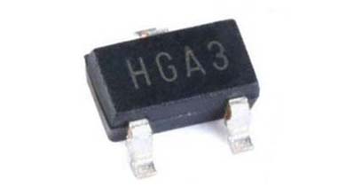
Initially, both of these regulators were specified as Microchip MCP1702 devices—SOT‑23A packaging for the 3.3V device and SOT‑89 packaging for the 5V device—for no other reason than that these were what I had on hand at the time. Both regulators are, nonetheless, available in both SOT‑23A and SOT‑89 packaging.
| SOT-23A | SOT-89 |
|---|---|
 |
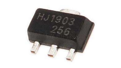 |
MCP1702 Voltage Regulator Packaging
But as with my boost converter design, I quickly discovered that there's more to a regulator, indeed more to a power circuit, than the output voltage. The Microchip Technology MCP1700 and MCP1702 series regulators have been fine for the 'smaller' processors that I've been using—the Arduino Pro Mini and ESP8266. But I very quickly ran into trouble with the more powerful processors, the ESP32 and Pi Zero, that drew more current, particularly the latter when booting.
The short of it is that the MCP170x series regulators are 250mA devices, and while this might be more than enough for the 'smaller' processors, or even things like the ESP32 when the boot process is complete, this limits their suitability in the present application.
Coincidentally, in the design of the BCS-A4a prototyping board, I had included an alternative regulator, the Microchip Technology MIC5219, which could be switched off when not in use. More importantly, in the present context, this regulator is rated at 500mA, a fact I only discovered after noting that the ESP32-WROOM-32 ran without any problem on boards configured with this regulator.
I had read all the relevant datasheets but, quite simply, I hadn't really appreciated the significance of much of what I was reading.
The other aspect of these regulators that I discovered the hard way was their drop-out characteristics. I could see that some of these devices were described as 'low drop-out' regulators, but I didn't really understand what this meant, or what impact the drop-out voltage would have, until the regulator in some of my board configurations actually started dropping out!
Once again, this practical experience gave [new] meaning to some of the table entries in the device datasheets—I look forward to the day when there's more in a datasheet that I undestand than not.
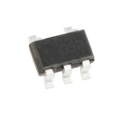
In working through my power supply problems, I looked at two other regulators that I'd noticed in circuits supporting ESP32 and Pi Zero processors respectively: the Diodes Incorporated AP2112 (3.3V) and STMicroelectronics LD1117 (3.3V/5V). Fortunately, the MIC5219 and AP2112 regulators share the same SOT-23-5 footprint and I have been able to accommodate both of these as options on a single board, where this is relevant.
| SOT-23-5 | SOT-223 |
|---|---|
 |
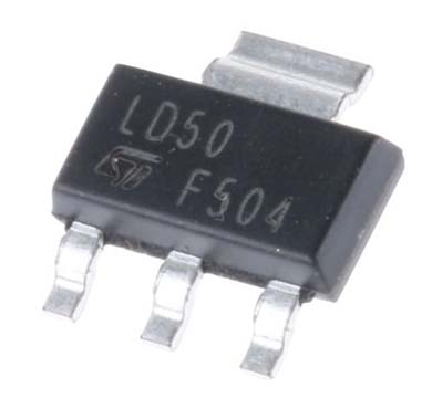 |
AP2112 (left) and LD1117 (right) Voltage Regulator Packaging
Some of the key characteristics of the regulator options described above are presented in the table below. Most of these regulators come in several output voltage ratings but, with the exception of the MCP1702 and LD1117, I have only ever used the 3.3V versions.
Voltage Regulator Characteristics
| Regulator | VDO | Imax | IQ | ISTD | Unit Price |
|---|---|---|---|---|---|
| mV | mA | µA | µA | A$ | |
| MCP1700 | 178 | 250 | 1.6 | $0.25 | |
| MCP1702 | 625 | 250 | 2.0 | $0.38 | |
| MIC5219 | 600 | 500 | 8 | 0.1 | $0.35 |
| CE6260 | 650 | 500 | 6 | 0.1 | $1.49 |
| AP2112 | 1000 | 600 | 55 | 0.1 | $0.30 |
| LD1117 | 1200 | 800 | 5000–10000 | $0.44 |
At first glance then, the MCP170x regulators appear to offer significantly better quiescent current characteristics than the others and on that basis would be the best candidates for battery powered applications. The MIC5219, CE6260 and AP2112 regulators, however, can all be disabled when not in use, each drawing only 0.1µA in that standby state, making them a potentially better choice in low-power applications where they can be disabled when not in use.
Given the price and availability of the Chipower Technology CE6260, I've never even tested this device. It is only included in my list because it is the regulator employed on most of the Heltec boards I have used.
While it draws a significant current in its own right, the LD1117 regulator supports a much higher current draw overall than the others and was the regulator I chose to use to power the [5V] Pi Zero, where the battery is used more in a UPS role than as a primary power source and power consumption is thus less of an issue.
Ultimately, however, I was worried that, given that a 5V/2.5A power supply is recommended for the Raspberry Pi Zero 2 W, the 800mA limit on the LD1117 would not be enough. The alternative, to support higher current draw, seemed to be a buck converter configuration, but I ultimately decided that venturing down that path was taking me too far away from my original objective, which was simply to provide battery back-up for a Pi Zero that would normally be powered through a USB connection.
So that's where I've now ended up, with a board that simply takes power from an 'external' USB connection, as distinct from the USB 'power' port provided on the Pi Zero, and provides battery back-up. The solar panel support is there just because I have it on most of my other power boards and it didn't involve any particular effort or cost to include it.
The 3.3V supply components were originally included to support 3.3V MCUs and any relevant sensors, but this need has effectively passed with all the other boards that I now have that are dedicated to this function. None of the related components need to be configured, but the connections remain in the current circuit 'just in case' some application pops up.

