

13095-BPHC PCB
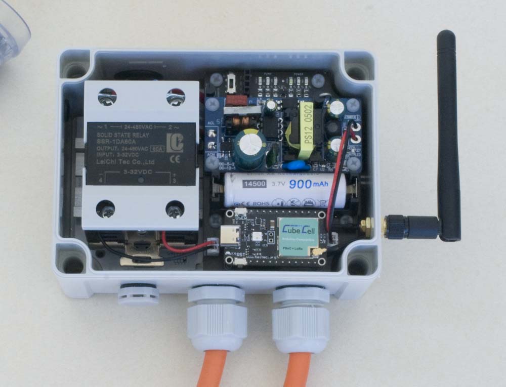
Board Layout
This board is designed to be used in a 'sandwich' configuration with the 13095-BP-R PCB in the Power Switch Node.
Further details pending
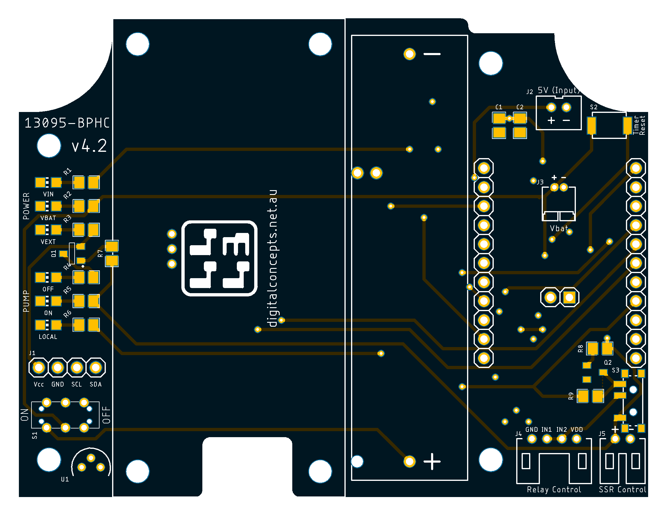
The various subsystems are identified in the board schematic and laid out as illustrated below:
| Top | Bottom |
|---|---|
 |
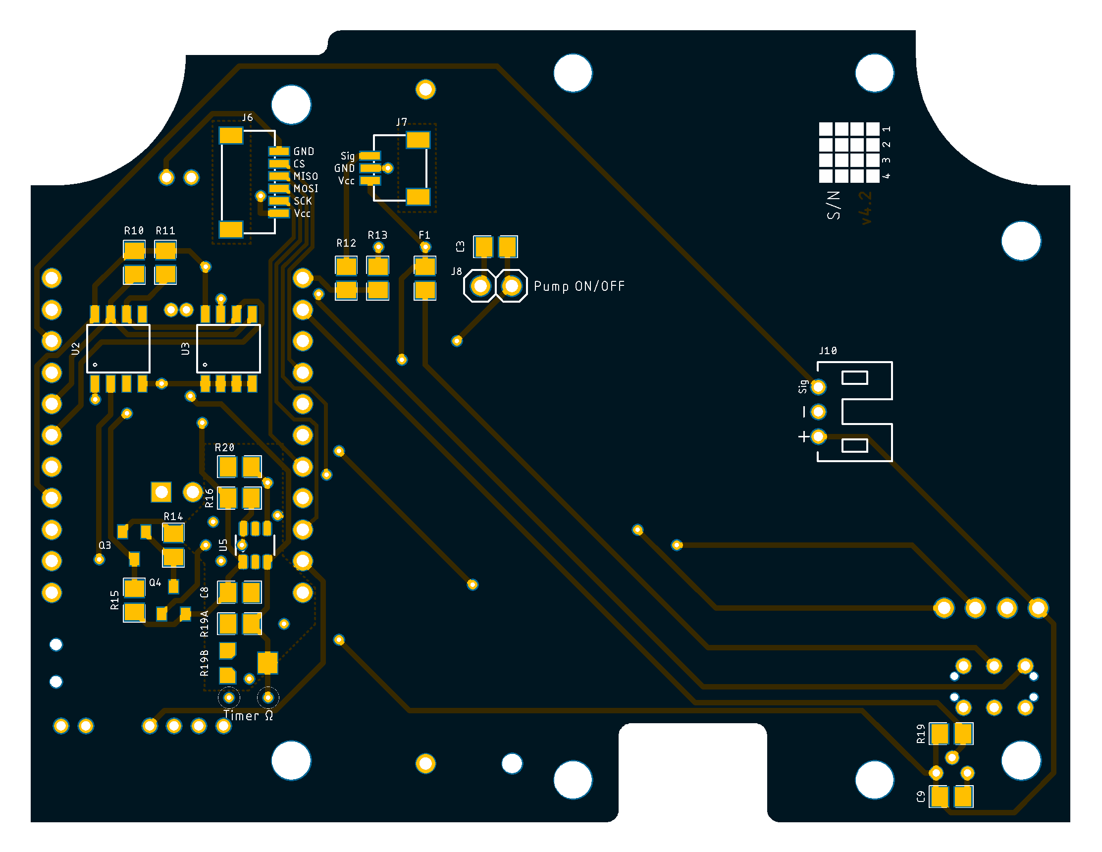 |
13095-BPHC [v4.2] PCB
See here for CAD and CAM files.
Configuration
See also the pages describing the Power Switch application and 13095‑BPHC board testing. The details discussed in the following sections, however, are of particular note.
GPIO Port Expander
As this application grew, several shortcomings of the CubeCell platform—originally chosen primarily for its physical size—were exposed, foremost being its pin limitations, both digital and analog. The present application hasn't needed more than the single ADC up to this point, but it quickly outgrew the six digital pins generally available on the CubeCell Dev Board. Stepping up to the CubeCell Dev Board Plus was not really an option without completely redesigning the board layout and moving to a larger enclosure.
This problem was resolved using an I2C-controlled PCA9536 GPIO port expander. Since the application already included an I2C bus, this provided an additional four digital ports, with minimal impact on board real estate. Only two of these ports are currently used, for the control of the relay and the relay and pump status LEDs.
Switching Circuits
To control the relay status LEDs through a single control signal, the red 'Relay OFF' LED is connected through a P-channel MOSFET that is controlled by the same signal that feeds directly into the green 'Relay ON' LED. When the control signal is HIGH, the green LED is switched on, the MOSFET is open and the red LED is switched off. When the control signal is LOW, the green LED is switched off and the MOSFET is closed, switching on the red LED by connecting it directly to Vcc.
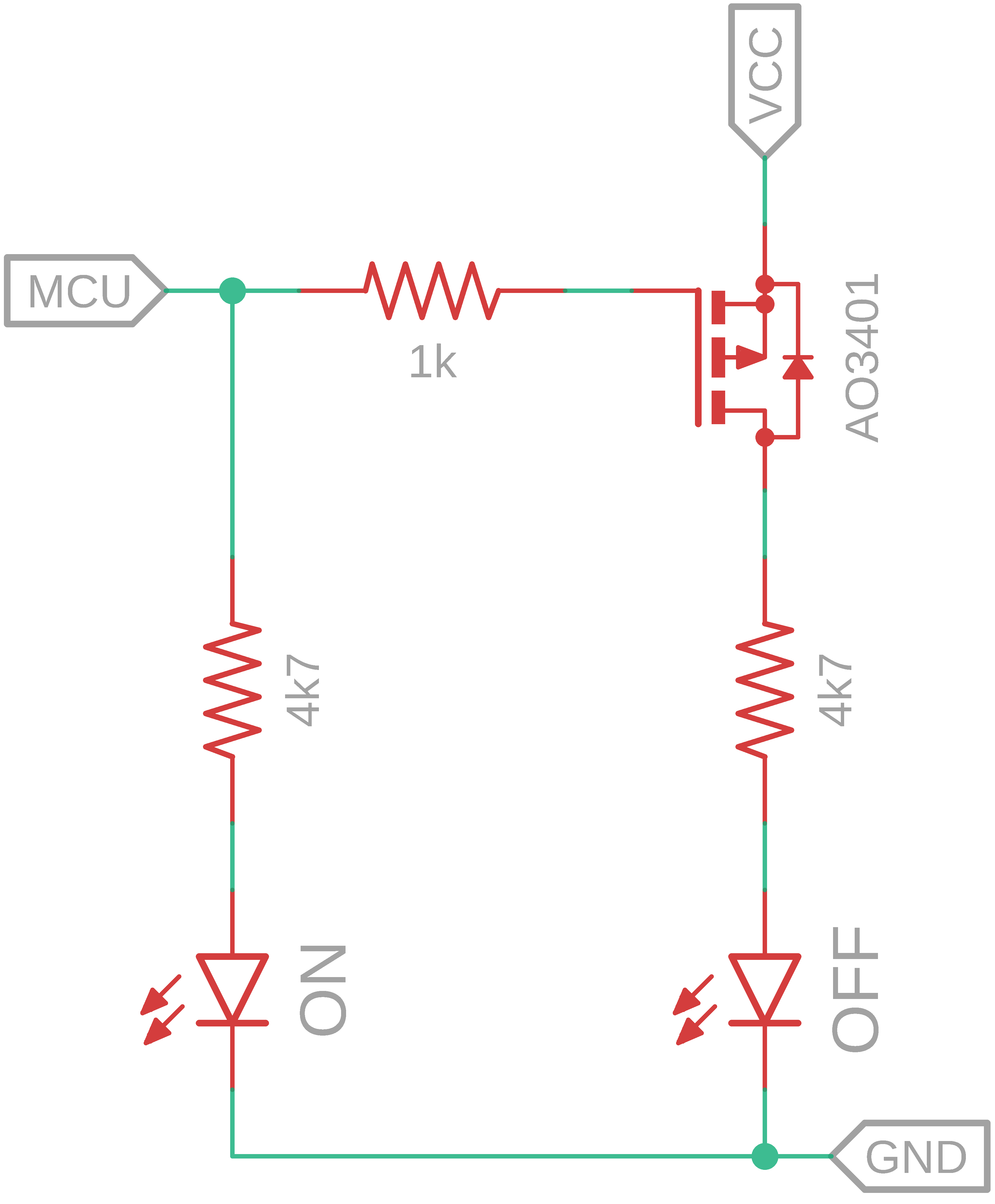
MOSFET ON-OFF LED Control Circuit
A similar problem surfaced when adding the ability to control a mechanical relay as an alternative to a solid state relay (SSR). The mechanical relay that I had purchased used the opposite control logic to that of the SSR. Some mechanical relays, I have since discovered, include the ability to configure the logic level used to close or switch ON the relay(s), but the one that I had did not.
All of the relays that I have seen do provide the ability to connect the output to either the closed or open side of the relay, so that the output in the relay's default, or normal state is ON or OFF respectively. So one solution to this problem would be to simply connect my circuit to the 'Normally Open' side of the relay. It's perhaps a fussy detail, but the relay output state is then not 'logically' reflected in it's onboard status LEDs—the LEDs are ON when the output is OFF, and vice versa.
To resolve this problem, the V4.0 and later boards include a 2-pole Relay Mode switch, one input of which connects directly to the control logic and the other through a simple logic inverter circuit, implemented using an NPN transistor as illustrated below. Switching between the two then allows the selection of direct or inverted relay control logic where this option is not available on the relay module itself.
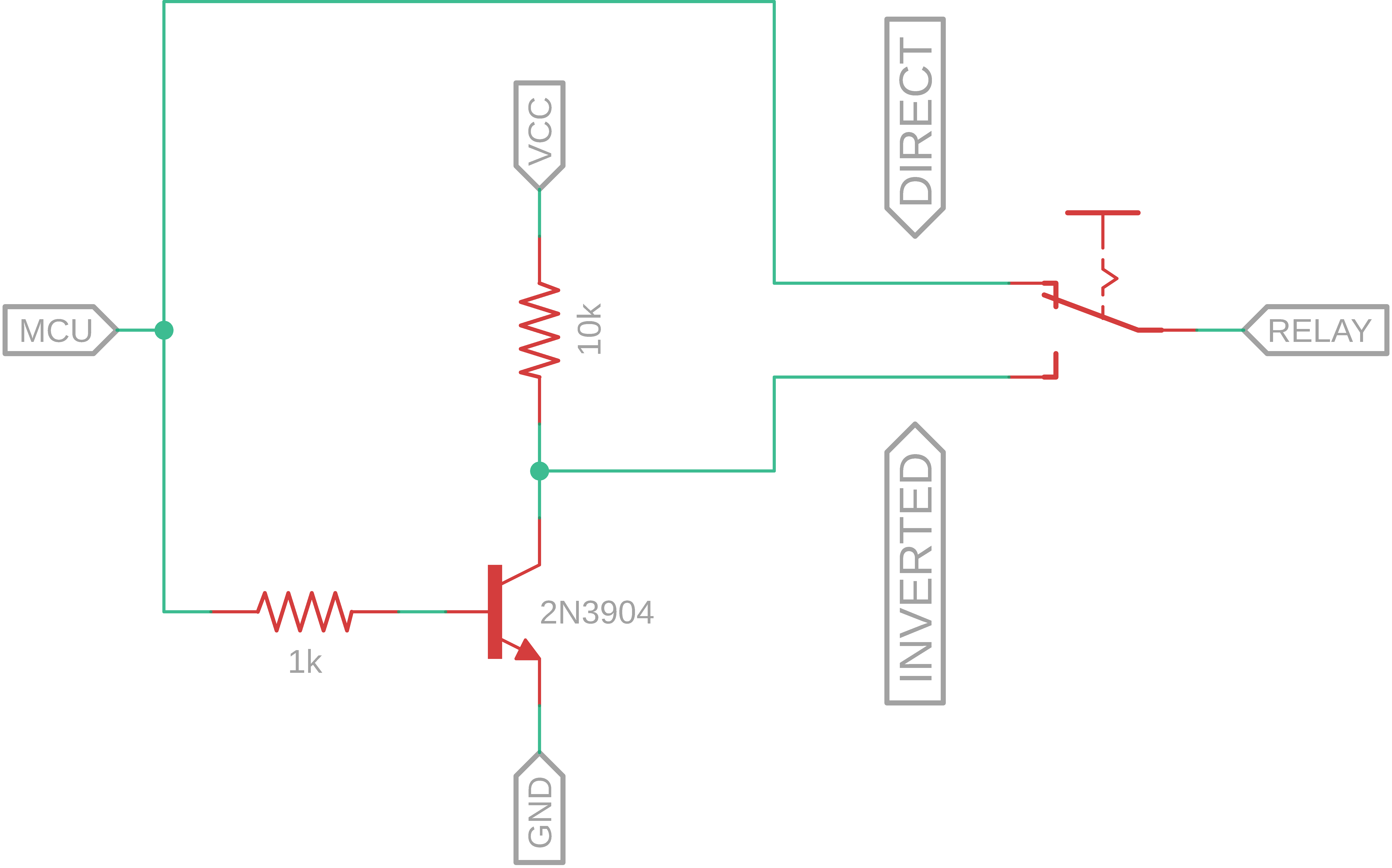
Relay Mode Circuit
Watchdog Timer
The watchdog timer circuit used on this board, which is discussed in detail on the Watchdog Timer page, is the variant that includes a reset button. In the present case, the reset button would rarely be used any time other than during initial set-up and it can be omitted without impacting the normal operation of the watchdog circuit.
Further details pending